Manufacturing method of active matrix substrate, active matrix substrate and liquid crystal display device

a technology of active matrix substrate and liquid crystal display device, which is applied in the direction of semiconductor devices, instruments, electrical devices, etc., can solve the problem that liquid crystal cannot be supplied with sufficient voltage, and achieve the effect of excellent properties and preferable application properties

Inactive Publication Date: 2008-12-09
SAMSUNG ELECTRONICS CO LTD
View PDF47 Cites 98 Cited by
  • Summary
  • Abstract
  • Description
  • Claims
  • Application Information

AI Technical Summary

Benefits of technology

[0012]The present invention has been achieved in consideration of these problems, and an object of the invention is to provide a novel technique which permits independent free selection of a substrate used in producing thin film devices, and a substrate (a substrate having preferable properties for application of a product) used in, for example, actual use of a product, and a completely new method of effectively manufacturing an active matrix substrate having excellent properties and a liquid crystal display device by using the technique.
[0037]This invention is different from invention (1) in that the intermediate layer is provided. The intermediate layer can comprise a single layer film of an insulator, such as an SiO2 film or the like, or a multilayered film comprising a laminate of an insulator and a metal. The intermediate layer functions to facilitate separation from the separation layer, protect the transistors from contamination during removal of the separation layer, ensure insulation properties of the transistors, and suppress irradiation of the transistors with laser light.
[0038]In forming the thin film transistors and the pixel electrodes on the original substrate before transfer, at least a portion of the insulator layer such as an interlayer insulation film or the like, which causes a problem in the later steps, is removed before the pixel electrodes are formed. In this case, the whole insulation film and intermediate layer below it are preferably removed at the same time from the viewpoint of prevention of a loss of the voltage applied to the liquid crystal. However, where the insulator layer remaining unremoved is thin, a sufficient voltage can be applied to the liquid crystal from the pixel electrodes. Therefore, at least a portion of the insulation film may be removed.
[0071](12) This invention provides an active matrix substrate manufactured by the method of manufacturing an active matrix substrate of any one of inventions (1) to (11). Since limitations due to the manufacturing conditions are eliminated so that the substrate can freely be selected, a novel active matrix substrate, which has not yet been realized, can be realized.(13) This invention provides a liquid crystal display device comprising an active matrix substrate manufactured by the method of manufacturing an active matrix substrate of any one of inventions (1) to (11). For example, it is possible to realize an active matrix type liquid crystal display device comprising a plastic substrate and having flexibility.

Problems solved by technology

If the insulation film has a large thickness, a large voltage loss occurs in this portion, and thus a sufficient voltage cannot be applied to a liquid crystal.

Method used


Image

  • Manufacturing method of active matrix substrate, active matrix substrate and liquid crystal display device
  • Manufacturing method of active matrix substrate, active matrix substrate and liquid crystal display device
  • Manufacturing method of active matrix substrate, active matrix substrate and liquid crystal display device

Examples


first embodiment

(First embodiment)

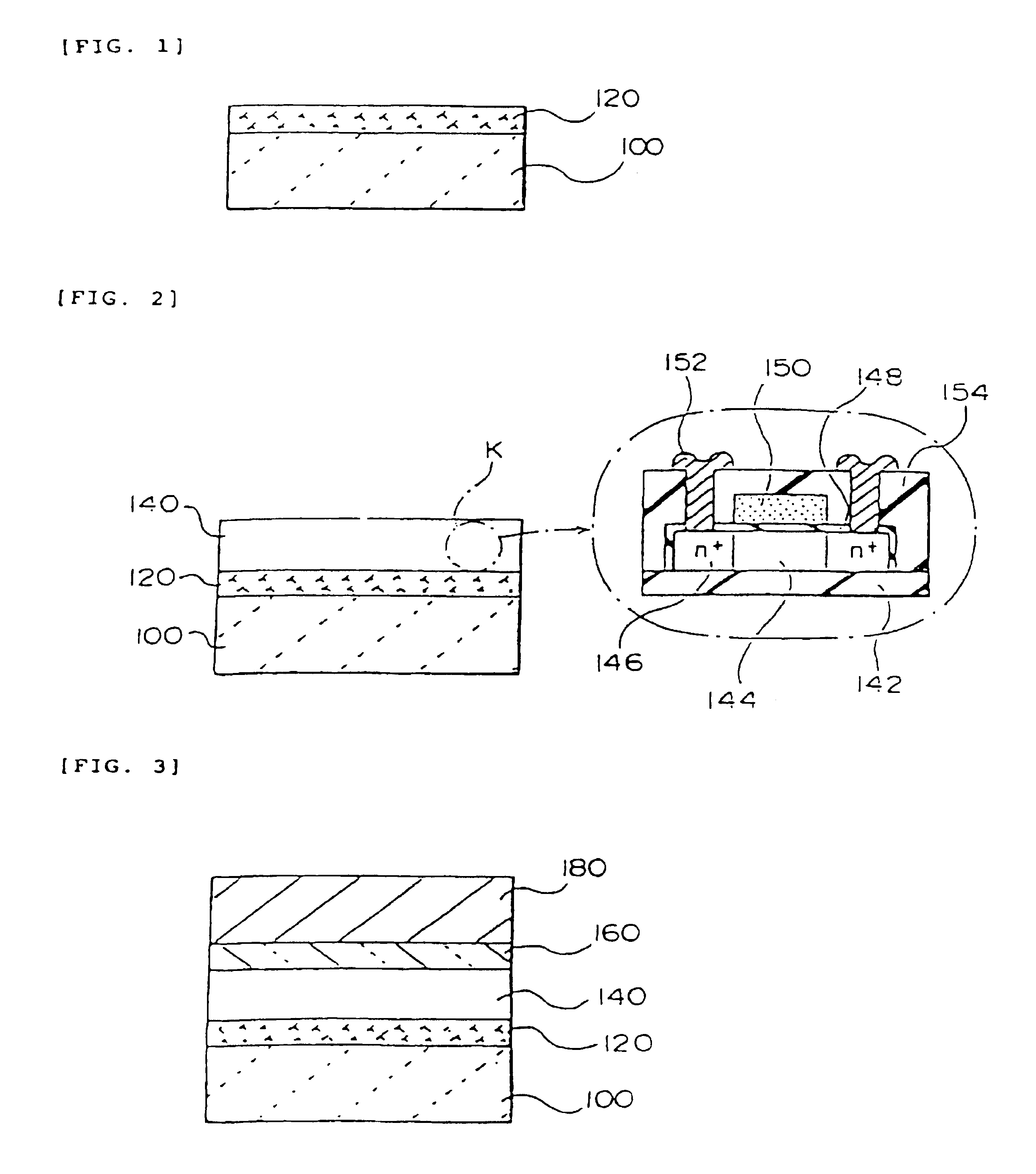
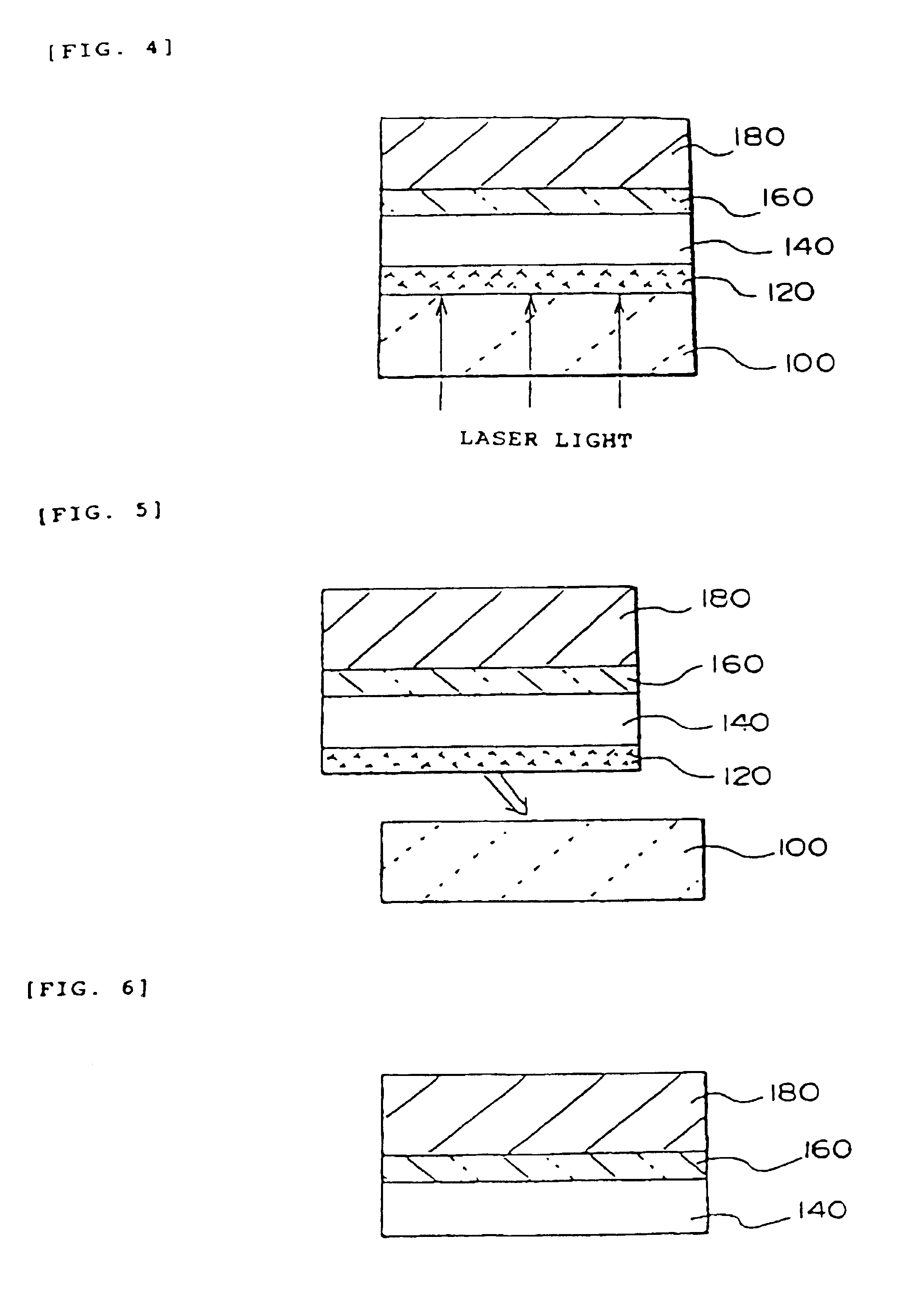
[0181]In this embodiment, an example of the process for manufacturing an active matrix type liquid crystal display device comprising an active matrix substrate, as shown in FIGS. 7, 8 and 9, using the thin film device transfer technique is described.

(Configuration of liquid crystal display device)

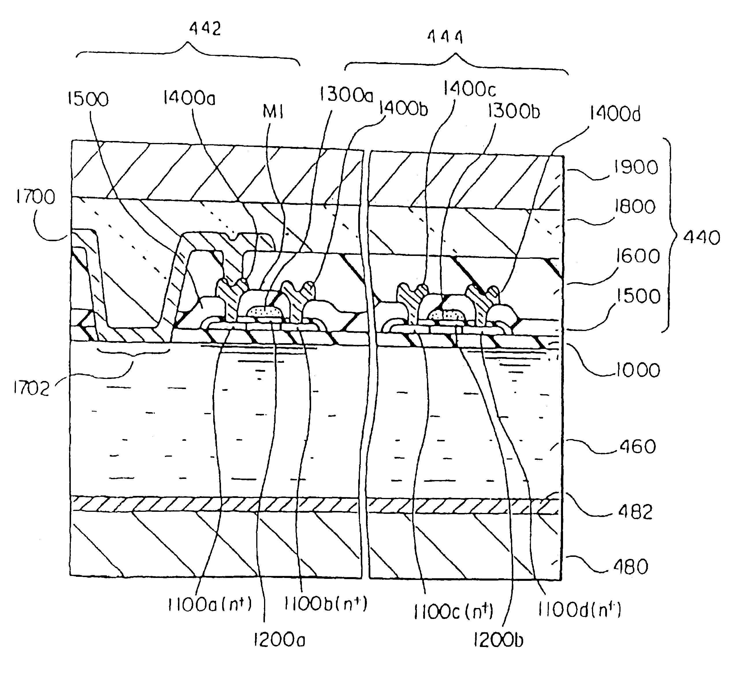
[0182]As shown in FIG. 7, an active matrix type liquid crystal display device comprises backlights 400, a polarizer 420, an active matrix substrate 440, a liquid crystal 460, an opposite substrate 480, and a polarizer 500. In the present invention, when a flexible substrate is used as each of the active matrix substrate 440 and the opposite substrate 480, a lightweight active matrix type liquid crystal panel having flexibility and resistance to shock can be realized as a reflective liquid crystal panel by using a reflecting plate in place of the illumination light sources 400.

[0183]The active matrix substrate 440 used in this embodiment is an active matrix substrate with a...

second embodiment

(Second embodiment)

[0215]FIGS. 18 and 19 are sectional views showing a device in accordance with a second embodiment of the present invention.

[0216]This embodiment is characterized in that the step of forming a color filter and a light shielding film (for example, a black matrix) is added after the step of forming the pixel electrode made of ITO or a metal to form an active matrix substrate with the color filter and the light shielding film (for example, a black matrix).

[0217]The case where the black matrix is used as the light shielding film is described below.

[0218]As the structure of an ordinary thin film transistor, a structure in which the color filter and the black matrix are formed on the pixel electrode cannot be used because the liquid crystal layer and the pixel electrode are separated.

[0219]However, in the present invention, a device is reverse to a normal device due to transfer, and thus the contact region between the pixel electrode and the liquid crystal layer is forme...

third embodiment

(Third embodiment)

[0224]FIG. 20 shows a section of the principal portion of a liquid crystal display device in accordance with a third embodiment of the present invention.

[0225]The liquid crystal display device shown in FIG. 20 is characterized in that a terminal (external connection terminal) 1404 (made of ITO or a metal) for connecting a driver IC 4200 is formed on the active matrix substrate through the same manufacturing steps as the pixel electrodes.

[0226]Namely, in the active matrix substrate, where the external connection terminal (for example, a terminal for connecting liquid crystal driving IC) is required, this terminal must be exposed to the surface.

[0227]Therefore, in the region where the external connection terminal is provided, the underlying insulation film (intermediate layer) and the insulator layer such as interlayer insulation film are moved.

[0228]However, the surface of the external connection terminal 1404 need not be exposed only in the same step as formation o...


PUM

PropertyMeasurementUnit
temperatureaaaaaaaaaa
light transmittanceaaaaaaaaaa

Abstract

A method of manufacturing an active matrix substrate is provided that uses a technique of transferring a thin film device. In forming thin film transistors and pixel electrodes on an original substrate before transfer, an insulator film such as an interlayer insulation film or the like, is previously removed before the pixel electrodes are formed. Further, the original substrate is separated by exfoliation to transfer the device to a transfer material to cause the pixel electrodes to partially appear in the surface or the vicinity of the surface of the device. This portion permits application of a voltage to a liquid crystal through the pixel electrode.

Description

[0001]This is one of two (2) reissue applications directed to various aspects of manufacturing method of active matrix substrate, active matrix substrate and liquid crystal display device described in U.S. Pat. No. 6,127,199. The first reissue application is application Ser. No. 10 / 263,070, filed Oct. 3, 2002. The second reissue application is the present application, which is a Divisional of application Ser. No. 10 / 263,070. As noted above, this is a Divisional of application Ser. No. 10 / 263,070, filed Oct. 3, 2002 now Re. 38,466 which is a reissue of U.S. Pat. No. 6,127,199, which corresponds to U.S. patent application Ser. No. 09 / 113,373 filed Jul. 10, 1998, which is a Continuation-In-Part of Application No. PCT / JP97 / 04110 filed Nov. 11, 1997.<?insert-end id="INS-S-00001" ?>CROSS-REFERENCE TO RELATED APPLICATIONS[0002]This application is a continuation-in-Part of international application PCT / JP97 / 04110, filed on Nov. 11, 1997, which claims priority from Japanese application...

Claims


Application Information

Patent Timeline
Patent Type & Authority Patents(United States)
IPC IPC(8): H01L21/00G02F1/1368H01L21/762H01L21/77H01L21/84H01L27/12
CPCG02F1/1368H01L21/76251H01L27/1214H01L27/1266G02F2001/13613H01L2221/68359H01L2924/13091H01L2224/76155H01L2924/01025H01L2924/01057H01L2924/01078H01L2924/01019H01L2224/24226G02F1/13613
Inventor INOUE, SATOSHISHIMODA, TATSUYA
Owner SAMSUNG ELECTRONICS CO LTD
Why Eureka
Try Eureka