Stable semiconductor storage device with pseudo storage unit

A technology of pseudo memory cells and storage devices, which is applied in the fields of semiconductor devices, semiconductor/solid-state device manufacturing, information storage, etc., and can solve the problems of prolonging the design and development cycle, etc.

Inactive Publication Date: 2007-08-29
MITSUBISHI ELECTRIC CORP
View PDF3 Cites 4 Cited by
  • Summary
  • Abstract
  • Description
  • Claims
  • Application Information

AI Technical Summary

Problems solved by technology

However, in this document, since the dummy memory cell is activated by the dummy word line, the dummy bit line is pulled down at a timing earlier than the activation timing of the normal memory cell.
Thus, for the offset, although the tolerance can be improved by equalizing the pull-down speed of a plurality of dummy memory cells, it is necessary to consider the difference in

Method used


Image

  • Stable semiconductor storage device with pseudo storage unit
  • Stable semiconductor storage device with pseudo storage unit
  • Stable semiconductor storage device with pseudo storage unit

Examples


Embodiment 1

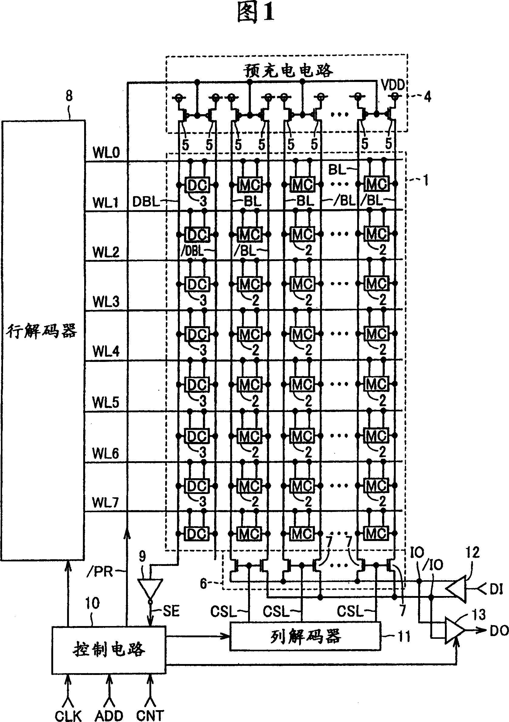
[0034] FIG. 1 is a circuit block diagram showing the overall configuration of an SRAM according to Embodiment 1 of the present invention. In FIG. 1 , the SRAM includes a memory cell array 1 , a precharge circuit 4 and a column selection gate 6 . The memory cell array 1 includes: a plurality of memory cells (MC) 2 configured in multiple rows (8 rows in the figure) and multiple columns, 8 word lines WL0-WL7 respectively arranged corresponding to the 8 rows, and 8 word lines WL0-WL7 respectively arranged corresponding to the multiple columns A plurality of bit line pairs BL, / BL. Each memory cell 2 is connected to a corresponding word line WL and a corresponding pair of bit lines BL, / BL, and stores one data signal.

[0035] In addition, memory cell array 1 includes 8 dummy memory cells (DC) 3 arranged in 8 rows and 1 column, and dummy bit line pairs DBL, / DBL. The dummy memory cell (DC) 3 is connected to the corresponding word line WL and the dummy bit line pair DBL, / DBL, and...

Embodiment 2

[0084] FIG. 23 is a circuit block diagram showing the overall structure of an SRAM according to Embodiment 2 of the present invention, for comparison with FIG. 1 . Referring to FIG. 23 , the difference between this SRAM and the SRAM in FIG. 1 is that a redundant memory cell array 41 is added, and the row decoder 8 is replaced with a row decoder 42 .

[0085] The redundant memory cell array 41 includes at least one row (one row in the figure) of dummy memory cells 3 , a plurality of memory cells 2 and spare word lines SWL. The row decoder 42 is provided with a programming circuit for programming a row address signal of a bad memory cell row. For example, when at least one memory cell 2 in the first row is defective, the row address signal of the memory cell row in the first row is programmed. When the row address signal of the memory cell row of the first row is input, the row decoder 42 raises the spare word line SWL to the "H" level of the selection level instead of the word...

Embodiment 3

[0088] FIG. 24 is a circuit block diagram showing the overall configuration of an SRAM according to Embodiment 3 of the present invention, for comparison with FIG. 1 . Referring to FIG. 24, the difference between the SRAM and the SRAM in FIG. 1 is that the memory cell array 1 and the pre-charging circuit 4 are replaced by the memory cell array 45 and the pre-charging circuit 46, respectively, and gate circuits 51-53 and "OR" gates are added. 54.

[0089] In the memory cell array 45 , two dummy memory cell columns are added to the end of the memory cell array 1 . One additional dummy memory cell column includes dummy bit line pair DBL, / DBL and 8 dummy memory cells 33 , and another added dummy memory cell column includes dummy bit line pair DBL, / DBL and 8 dummy memory cells 35 .

[0090] The precharge circuit 46 is to add 4 P channel MOS transistors 5 in the precharge circuit 4. The 4 P channel MOS transistors 5 are respectively connected to one end of the added 4 dummy bit l...


PUM


Abstract

The dummy cell of the SRAM corresponds to a normal memory cell of which first and second P-channel MOS transistors for loading are replaced by the first and the second N-channel MOS transistors, of which gate and source are provided with power supply potential and ground potential, respectively. When a word line rises to 'H' level, third and fourth N-channel MOS transistors for accessing are rendered conductive, to pass current from dummy bit line to a line of ground potential via the third N-channel MOS transistor, the first N-channel MOS transistor, and a fifth N-channel MOS transistor for driving. Accordingly, speed of potential decrease of the dummy bit line may be faster than that of bit line. Hence, operational timing can easily be optimized, and operational margin can be increased.

Description

technical field [0001] The present invention relates to a static semiconductor memory device, in particular, to a memory cell having a memory cell disposed at the intersection of a word line and a first and second bit line and a memory cell disposed at the intersection of the word line and the first and second dummy bit line A static semiconductor memory device of a dummy memory cell. Background technique [0002] Conventionally, in order to achieve high speed and low power consumption of a static random access memory (hereinafter referred to as SRAM), a method using a dummy memory cell has been proposed. For example, Japanese Patent Application Laid-Open No. 11-339476 discloses a method for setting dummy memory cells. When the word line corresponding to the address signal is at a selection level, the dummy memory cells and normal memory cells are simultaneously activated to output a prescribed readout signal. According to this method, when the word line is at the selection...

Claims


Application Information

Patent Timeline
IPC IPC(8): G11C11/34G11C11/41G11C11/419H01L21/8244H01L27/11
CPCG11C11/419G11C11/41
Inventor 渡边哲也新居浩二中濑泰伸
Owner MITSUBISHI ELECTRIC CORP
Why Eureka
Try Eureka