

Fast semiconductor heat-treating facility with vertical heat treating chamber
A rapid heat treatment, semiconductor technology, applied in semiconductor/solid-state device manufacturing, electrical components, circuits, etc., can solve the problems of large footprint and difficult to control the heating and cooling process of semiconductor wafers
- Summary
- Abstract
- Description
- Claims
- Application Information
AI Technical Summary
Problems solved by technology
Method used
Image

Examples
Embodiment Construction
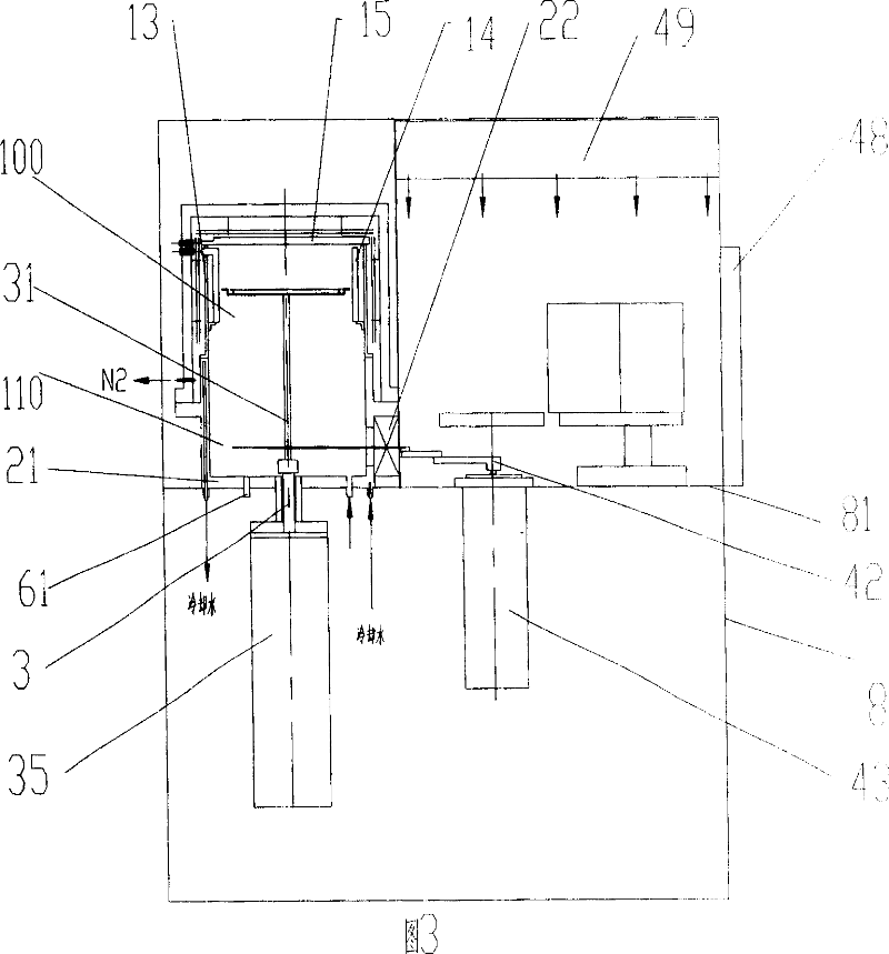
[0075] Fig. 3 is a schematic diagram of a semiconductor rapid heat treatment equipment with a vertical heat treatment chamber according to the present invention. Fig. 4 is a schematic structural view of the vertical cylindrical heat treatment chamber in Fig. 3 . Fig. 5 is a schematic diagram of the cassette-to-cassette pick-and-place robot subsystem in Fig. 3 . Fig. 6 is a schematic diagram of a direct current flat graphite heater. Fig. 7 is a schematic diagram of a direct current cylindrical graphite heater.
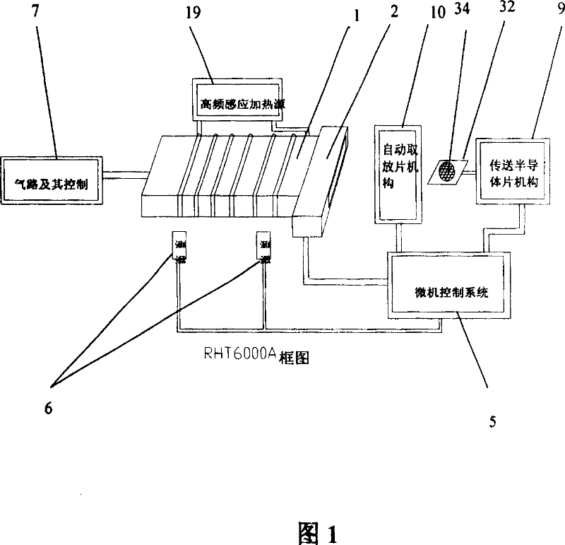
[0076] The semiconductor rapid heat treatment equipment with vertical heat treatment chamber mainly includes: vertically arranged heat treatment chamber 1, wafer loading chamber 2, semiconductor wafer lifting mechanism 3; also includes a cassette-to-cassette three-folding arm robot subsystem 4 , Microcomputer control subsystem 5, temperature measurement and control subsystem 6, gas circuit device 7, heating power supply 19.
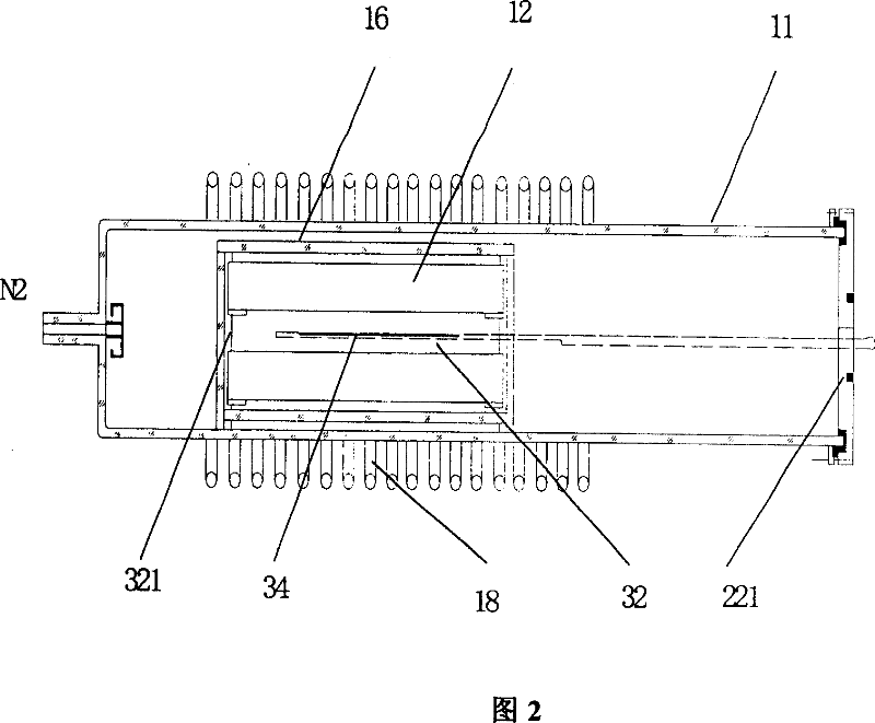
[0077] The heat treatment chamber mainly ...
PUM
 Abstract
Description
Claims
Application Information