Bridging chip package structure

A technology of chip packaging structure and manufacturing method, applied in semiconductor/solid-state device manufacturing, semiconductor/solid-state device components, semiconductor devices, etc.

Active Publication Date: 2008-01-23
ADVANCED SEMICON ENG INC
View PDF5 Cites 0 Cited by
  • Summary
  • Abstract
  • Description
  • Claims
  • Application Information

AI Technical Summary

Problems solved by technology

In order to solve the defects of the existing chip packaging structure and its manufacturing method, relevant manufacturers have tried their best to

Method used


Image

  • Bridging chip package structure
  • Bridging chip package structure
  • Bridging chip package structure

Examples


Embodiment Construction

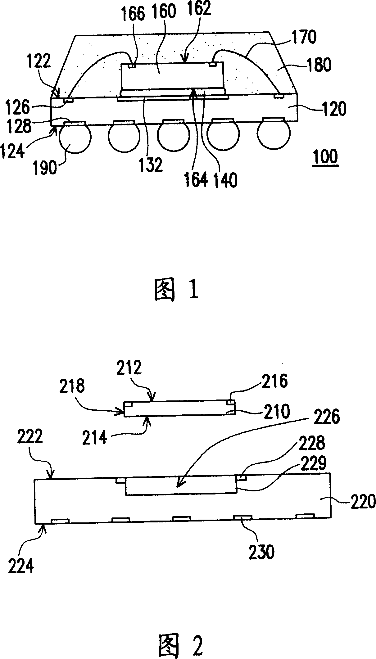
[0119] The specific structure, manufacturing method, steps, features and effects of the bridge-type chip packaging structure and its manufacturing method according to the present invention will be described in detail below with reference to the accompanying drawings and preferred embodiments.

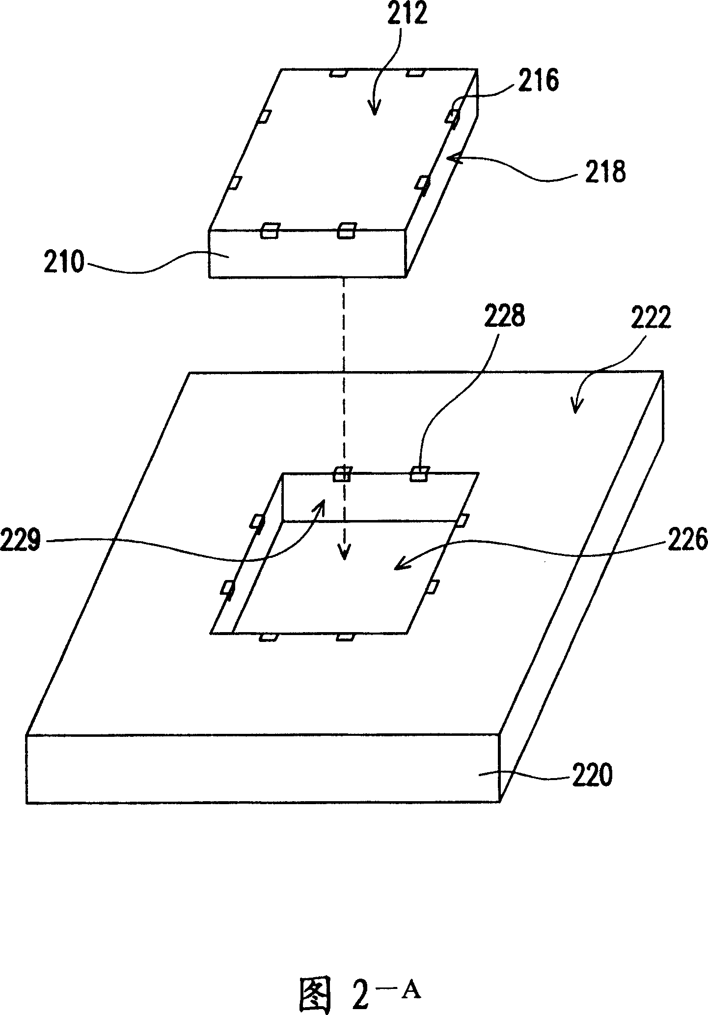
[0120] Please refer to FIG. 2 to FIG. 7 , which are schematic cross-sectional views of a chip packaging process according to the first preferred embodiment of the present invention. First, please refer to FIG. 2 and FIG. 2A , wherein FIG. 2A is a three-dimensional schematic view of the chip and the substrate in FIG. 2 . In the chip packaging process of the present invention, a chip 210 and a substrate 220 are provided first. The substrate 220 has a first surface 222 and a corresponding second surface 224. The substrate also has a recessed portion 226 and a plurality of substrate contacts 228. , 230, wherein the recessed portion 226 and the substrate contact 228 are located on the first ...


PUM


Abstract

The invention relates to a seal structure of chip of bridging-typed and its manufacture method, at last including a substrate, a chip and at least a conductor; the substrate has a first surface and its corresponding second surface, a depressed section and at least a contact of substrate, whose contact is on the first surface of substrate. The chip has a active surface and at least a contact of substrate which is on the active surface of chip. The chip is in the depressed section of substrate, whose at least one sidewall is near the depressed section, the active surface of chip and the first plane of substrate are installed for the public plane. Conductor is extending on the active surface of chip and the first plane on substrate, linking the contact of chip to that of substrate. The invention can shorten the distance between chip and substrate, increasing the electrical property efficiency of chip structure, which is more suitable for practical use and has use value in industry.

Description

technical field [0001] The present invention relates to a chip package structure and a manufacturing method thereof, in particular to a bridge connection type of chip package and process thereof which can improve electrical performance. Background technique [0002] In recent years, with the rapid development of electronic technology, high-tech electronic products have also come out one after another, so more humanized and functional electronic products are constantly being introduced. However, all kinds of products are designed towards the trend of light, thin, short and small. To provide more convenient and comfortable use. In the completion of an electronic product, electronic packaging plays an important role. There are generally three common ways for the electrical connection between the chip and the carrier. The first is wire-bonding, and the second is The method is tape automated bonding (TAB), and the third method is flip chip. As far as the wire-bonding method is ...

Claims


Application Information

Patent Timeline
IPC IPC(8): H01L23/12H01L23/48H01L21/50
CPCH01L24/24H01L2224/48091H01L2224/73265H01L2224/24H01L2924/00014H01L2924/00012
Inventor 洪志斌
Owner ADVANCED SEMICON ENG INC
Why Eureka
Try Eureka