
Narrow-pitch connector, electrostatic actuator, piezoelectric actuator, ink jet head

A narrow-pitch, connector technology, applied in the field of electronic devices and inkjet printers, can solve the problems of fine wiring 9 fusing and other problems, and achieve the effect of easy removal

Inactive Publication Date: 2008-01-30
SEIKO EPSON CORP
View PDF6 Cites 0 Cited by
  • Summary
  • Abstract
  • Description
  • Claims
  • Application Information

AI Technical Summary

Problems solved by technology

Therefore, when static electricity is generated in the air, the fine wiring 9 of the semiconductor device 3 is charged with static electricity, and the above-mentioned process is repeated, so there is also a problem that the fine wiring 9 is fused.

Method used


Image

  • Narrow-pitch connector, electrostatic actuator, piezoelectric actuator, ink jet head
  • Narrow-pitch connector, electrostatic actuator, piezoelectric actuator, ink jet head
  • Narrow-pitch connector, electrostatic actuator, piezoelectric actuator, ink jet head

Examples


Embodiment Construction

[0089] Embodiment 1

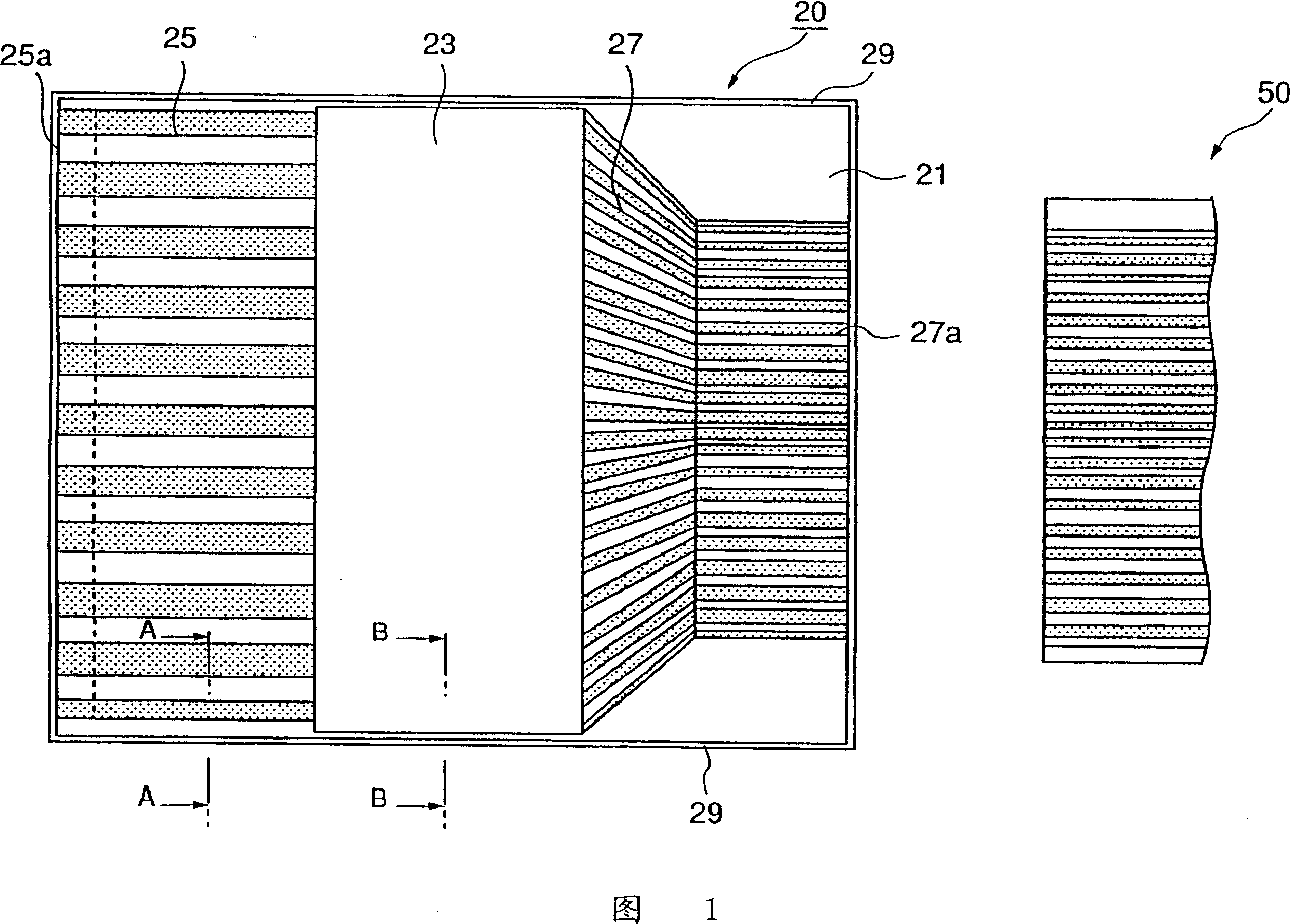
[0090]Fig. 1 is a plan view of a connector for a narrow pitch according to Embodiment 1 of the present invention. In the narrow-pitch connector 20, as shown in FIG. 1, an input wiring 25 and an output wiring 27 are formed on a substrate 21 made of single crystal silicon via an insulating layer, and a driver IC 23 is mounted. The ends of the input wiring 25 and the output wiring 27 become terminal electrodes 25a and 27a, respectively. In addition, the number of wirings and the wiring pitch on the input side and output side are changed.

[0091] In addition, the number of terminal electrodes 25a, 27a differs with the connection object 50 connected to the output side. In the case of the electrostatic actuator in which the object 50 is attached to the print head, it varies depending on the number of objects. However, it may be several tens or more on the input side and several hundred on the output side.

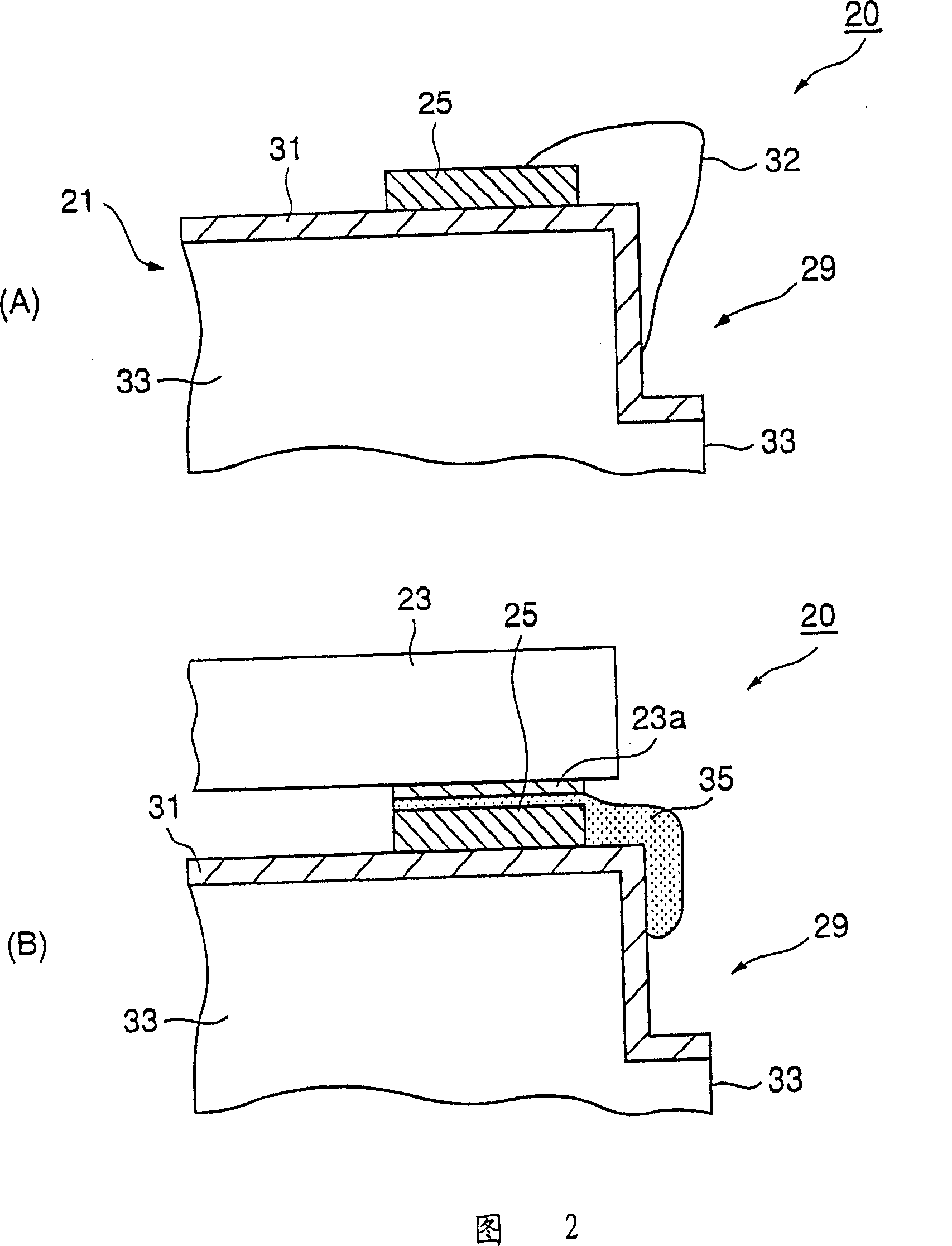
[0092] A step 29 recessed from the surface to the bottom ...


PUM


Abstract

A manufacturing method of semiconductor devices, micromachines such as semiconductor device, narrow pitch connectors, electrostatic actuators or piezoelectric actuators, and ink jet heads, ink jet printers, liquid crystal panels, and electronic appliances, including them characterized in that short circuit due to dusts floating in the air will not take place. In a method where a silicon wafer (30) undergoes dicing to manufacture semiconductor devices (20), a groove (30a) covered by an insulating layer and spanning a dicing line is formed in the above described silicon wafer, and the silicon wafer undergoes dicing along the dicing line.

Description

[0001] This application is a divisional application. The application number of the parent case is 00800468.4. The prior application number of this application is JP11-094074, and its prior date is March 31, 1999. Technical field [0002] The present invention relates to a manufacturing method of a semiconductor device, a semiconductor device, a connector for a narrow pitch, an electrostatic actuator including the connector for a narrow pitch, a piezoelectric actuator, a micromachine, a liquid crystal panel, and the electrostatic actuator, a piezoelectric The inkjet head of the actuator, the inkjet printer equipped with the inkjet head, and the electronic device. Background technique [0003] Conventionally, it has been known to form an insulating layer on a single crystal silicon wafer (hereinafter referred to as a silicon wafer), and simultaneously use the CVD method (or sputtering method) and etching to form wiring on the upper surface of the insulating layer to manufacture semi...

Claims


Application Information

Patent Timeline
Patent Type & Authority Patents(China)
IPC IPC(8): H01L23/48H01L23/52H01L23/12H01R24/00H01L41/08B41J2/045B81B1/00B81B7/00H01L21/78H01L23/552H01L23/58H01R31/06H02N2/04
CPCH01R31/06H01R12/7076B81B2207/99H01L23/585H01L21/78H01L23/552H01R23/6806H01R12/62H01L2924/15173H01L2924/0002H01L2924/00H10N30/00
Inventor 佐藤英一
Owner SEIKO EPSON CORP
Features
  • Generate Ideas
  • Intellectual Property
  • Life Sciences
  • Materials
  • Tech Scout
  • Unparalleled Data Quality
  • Higher Quality Content
  • 60% Fewer Hallucinations
Learn More