Electrostatic chuck for accelerating wafer etching uniformity

An electrostatic chuck and uniform technology, applied in the field of microelectronics, can solve the problems of affecting the heat conduction of the electrostatic chuck to the edge of the wafer, affecting the etching rate of the plasma to the wafer, difficult to control the temperature of the edge of the wafer, etc. Controllable and uniform effect

Active Publication Date: 2008-02-20
BEIJING NAURA MICROELECTRONICS EQUIP CO LTD
View PDF3 Cites 0 Cited by
  • Summary
  • Abstract
  • Description
  • Claims
  • Application Information

AI Technical Summary

Problems solved by technology

During the etching reaction process, the electrostatic chuck of the traditional structure has adverse effects on the wafer in two aspects:
[0004] (1) The edge area of ​​the electrostatic chuck 1 is in contact with the convex ring of the focus ring 4, which affects the heat conduction of the electrostatic chuck to the edge of the wafer, makes it difficult to control the temperature of the edge of the wafer, and indirectly affects the etching rate of the plasma to the wafer
[0005] (2) Due to the formation of steps in the area a at the edge of the electrostatic chuck, the capacitance value between the electrostatic chuck and the edge area of ​​the wafer is reduced relative to the part where the wafer is in full contact with the electrostatic chuck, increasing the impedance
In this way, the energy coupled to the edge of the wafer by radio frequency RF is reduced compared with the energy coupled to the central part, resulting in the inhomogeneity of plasma etching

Method used


Image

  • Electrostatic chuck for accelerating wafer etching uniformity
  • Electrostatic chuck for accelerating wafer etching uniformity

Examples


Embodiment Construction

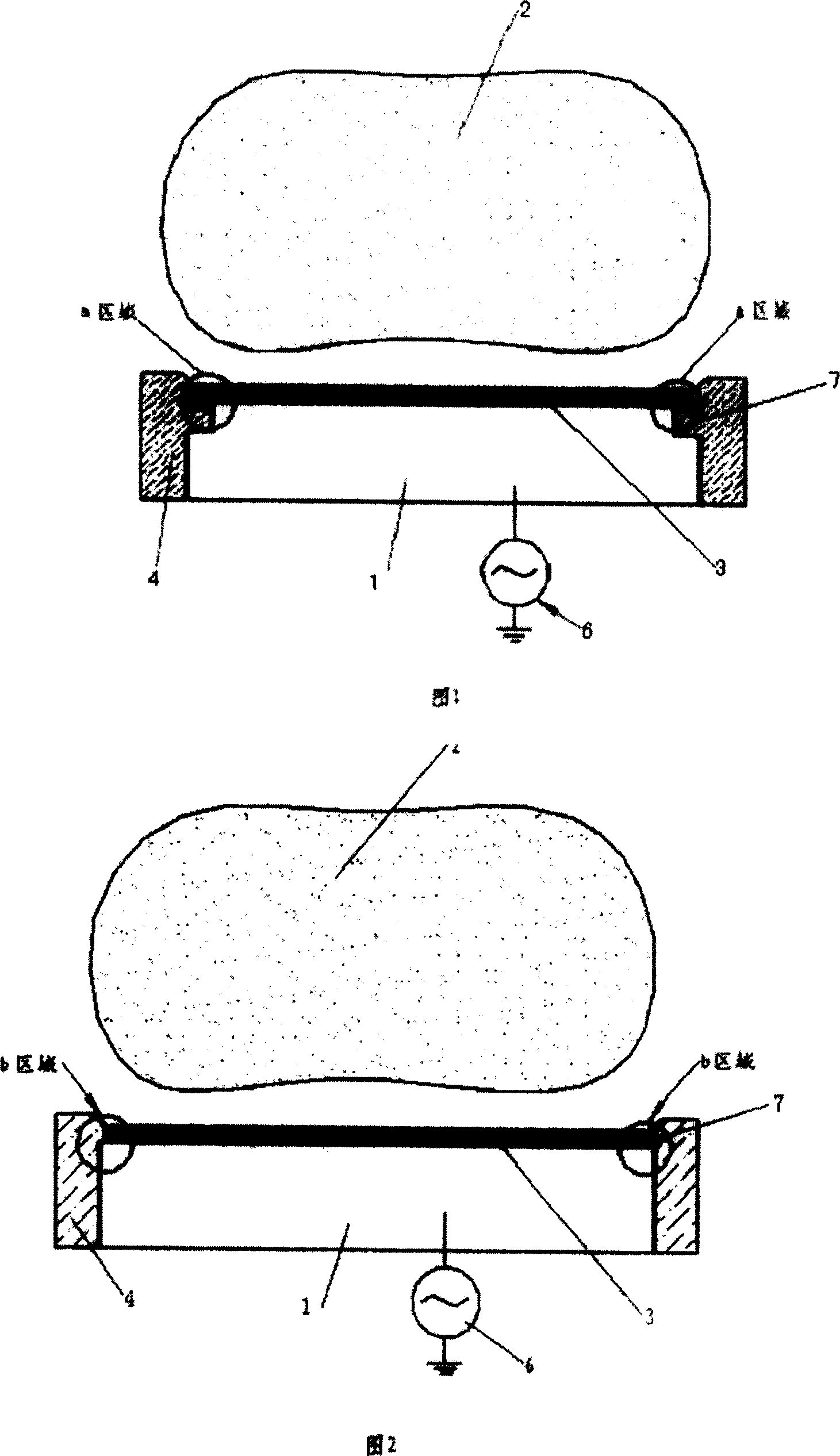
[0023] The specific implementation of the electrostatic chuck for promoting uniform wafer etching of the present invention will be further described in detail below in conjunction with the accompanying drawings, but it is not used to limit the protection scope of the present invention.

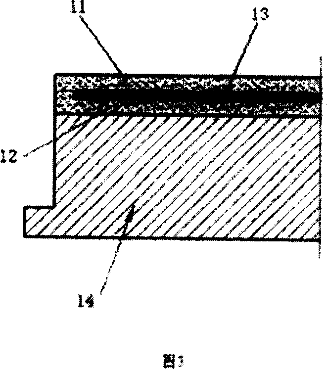
[0024] See Figure 2. The electrostatic chuck for promoting uniform wafer etching of the present invention includes an electrostatic chuck 1 and a focus ring 4 fitted on the outer circumference of the electrostatic chuck 1 , and a convex ring 7 integrated with the focus ring 4 is provided. Wherein the electrostatic chuck 1 has no boss on it, it is a plane, and the diameter of its upper surface is 2 mm larger than the diameter of the wafer 3 to be etched, and the range is 0.5-5 mm. Both are feasible; the lower surface of the protruding ring 7 cooperates with the upper surface of the electrostatic chuck 1 to protect the exposed part of the electrostatic chuck. In the present invention, a plurali...


PUM

PropertyMeasurementUnit
diameteraaaaaaaaaa
thicknessaaaaaaaaaa
thicknessaaaaaaaaaa

Abstract

The related static chuck benefit to evenness of wafer etching comprises a static chuck with diameter of top surface larger than the target wafer, and a focus ring matched round the chuck with an integrated convex ring with lower surface matched to the chuck top surface. The benefits of this invention comprises: effective temperature control to improve the temperature controllability of wafer edge, more stability on impedance between the chuck and the wafer, and more evenness on dc bias formed by RF to produce more even plasma.

Description

technical field [0001] The invention relates to the technical field of microelectronics, in particular to an electrostatic chuck for promoting uniform wafer etching by controlling the temperature of the wafer edge region and improving the radio frequency RF at the wafer edge. Background technique [0002] During the whole process of etching, the wafer is adsorbed and fixed by the electrostatic chuck (ESC) in the lower electrode system, and the radio frequency RF is passed into the electrostatic chuck, so that the radio frequency RF will form a DC bias (DC bias voltage) on the wafer. ). This facilitates the etching reaction of the plasma to the wafer. At the same time, the electrostatic chuck will control the temperature of the wafer to promote the uniformity of wafer etching. The upper and lower parts of the electrostatic chuck are insulating layers, and the middle part is provided with an electrode layer. When a DC voltage is applied to the electrode layer, different cha...

Claims


Application Information

Patent Timeline
Patent Type & Authority Patents(China)
IPC IPC(8): H01L21/683H01L21/67H01L21/3065H01L21/00C23F4/00
Inventor 孙亚林
Owner BEIJING NAURA MICROELECTRONICS EQUIP CO LTD
Why Eureka
Try Eureka