Combined probe for integrated circuit test

A technology of integrated circuits and combined probes, which is applied in the direction of electronic circuit testing, single semiconductor device testing, and parts of electrical measuring instruments. It can solve the problems of inconvenient maintenance and achieve convenient maintenance, simple and mature technology, and wide application. Effect

Active Publication Date: 2008-11-05
武汉精毅通电子技术有限公司
View PDF9 Cites 0 Cited by
  • Summary
  • Abstract
  • Description
  • Claims
  • Application Information

AI Technical Summary

Problems solved by technology

In addition, if the test structure made of the above two probes has quality problems and needs to replace a certain probe, the entire structure must be disassembled to replace it, which is inconvenient for maintenance.

Method used


Image

  • Combined probe for integrated circuit test
  • Combined probe for integrated circuit test
  • Combined probe for integrated circuit test

Examples


Embodiment Construction

[0023] The preferred embodiments shown in the accompanying drawings will be described in further detail below.

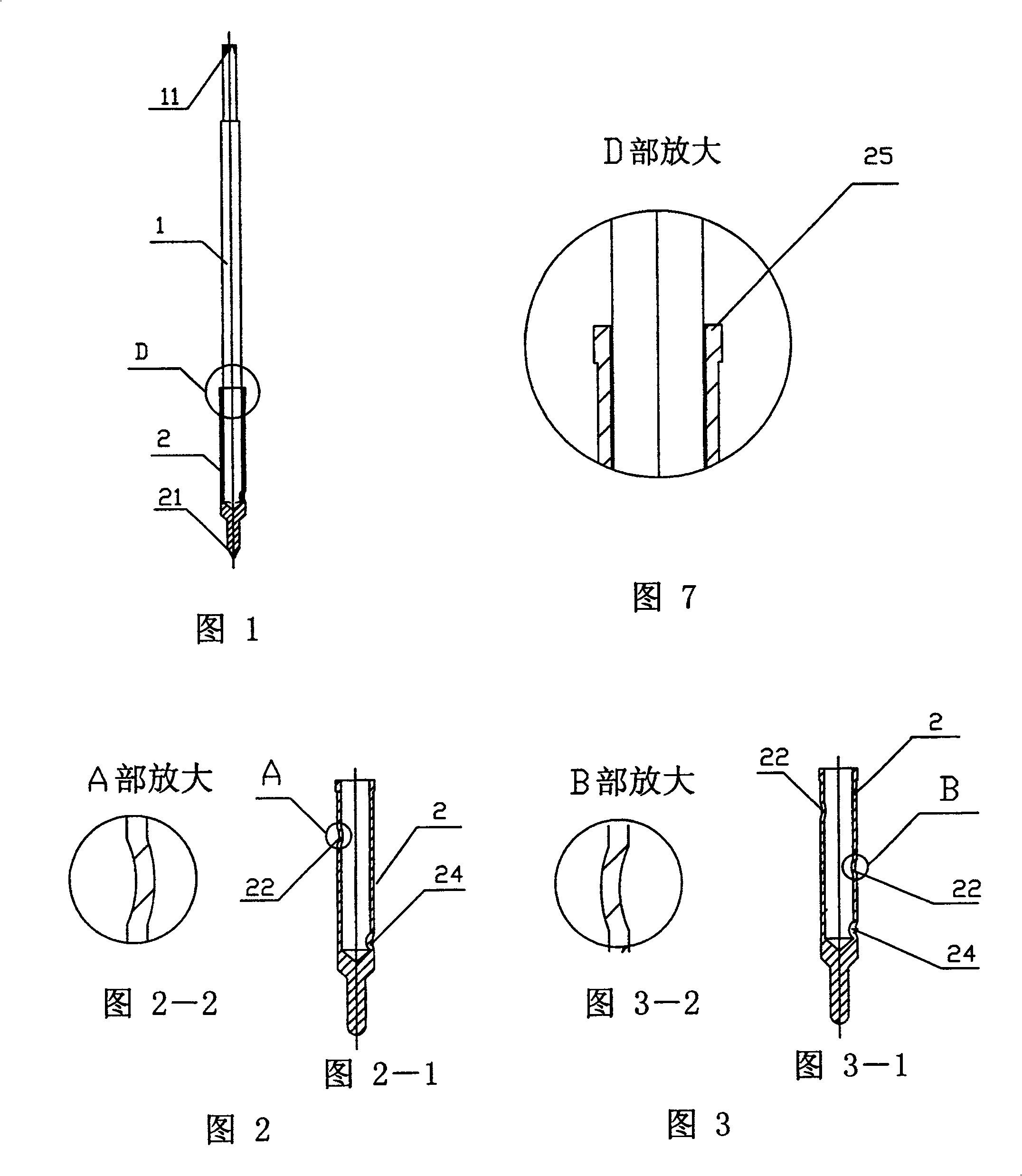
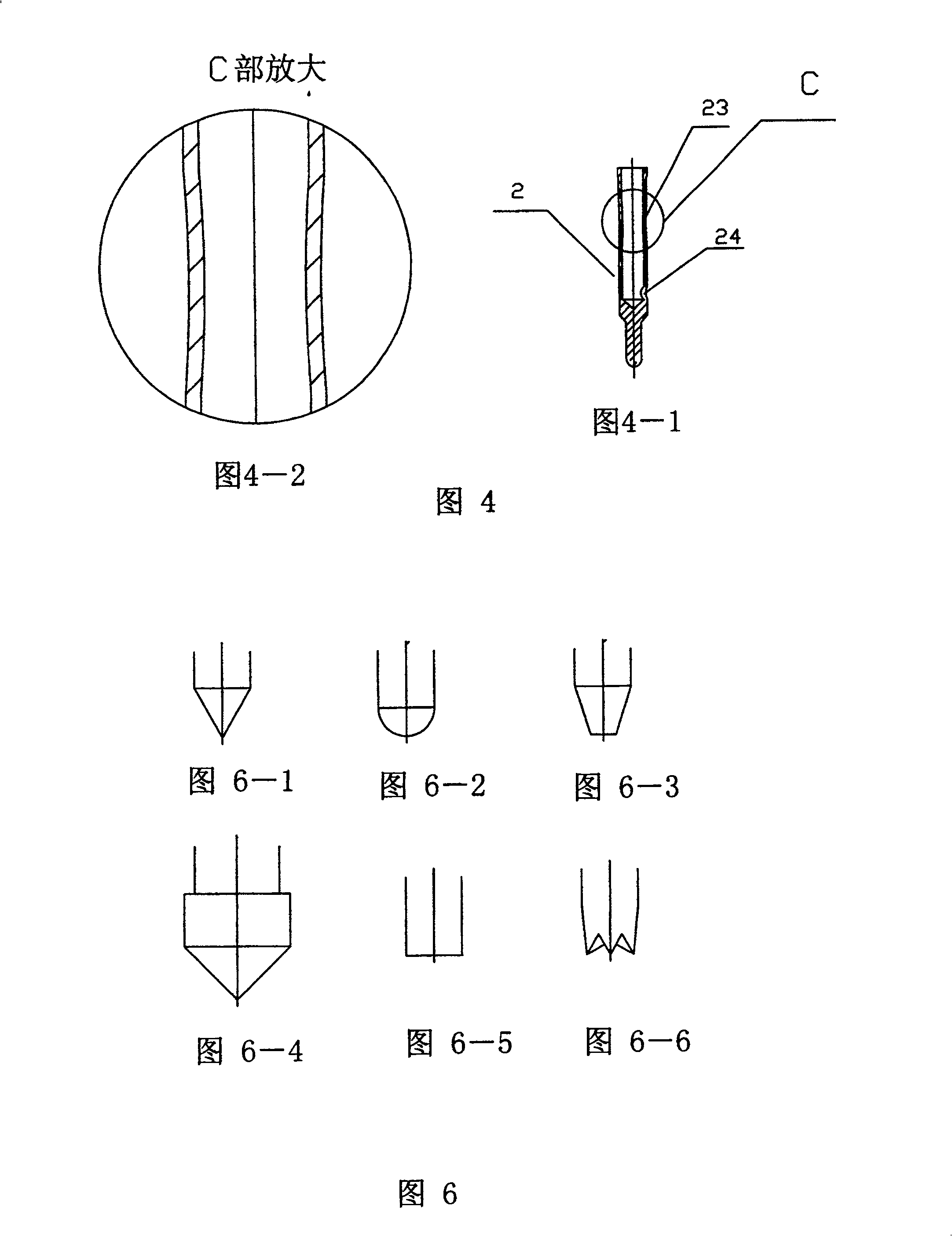
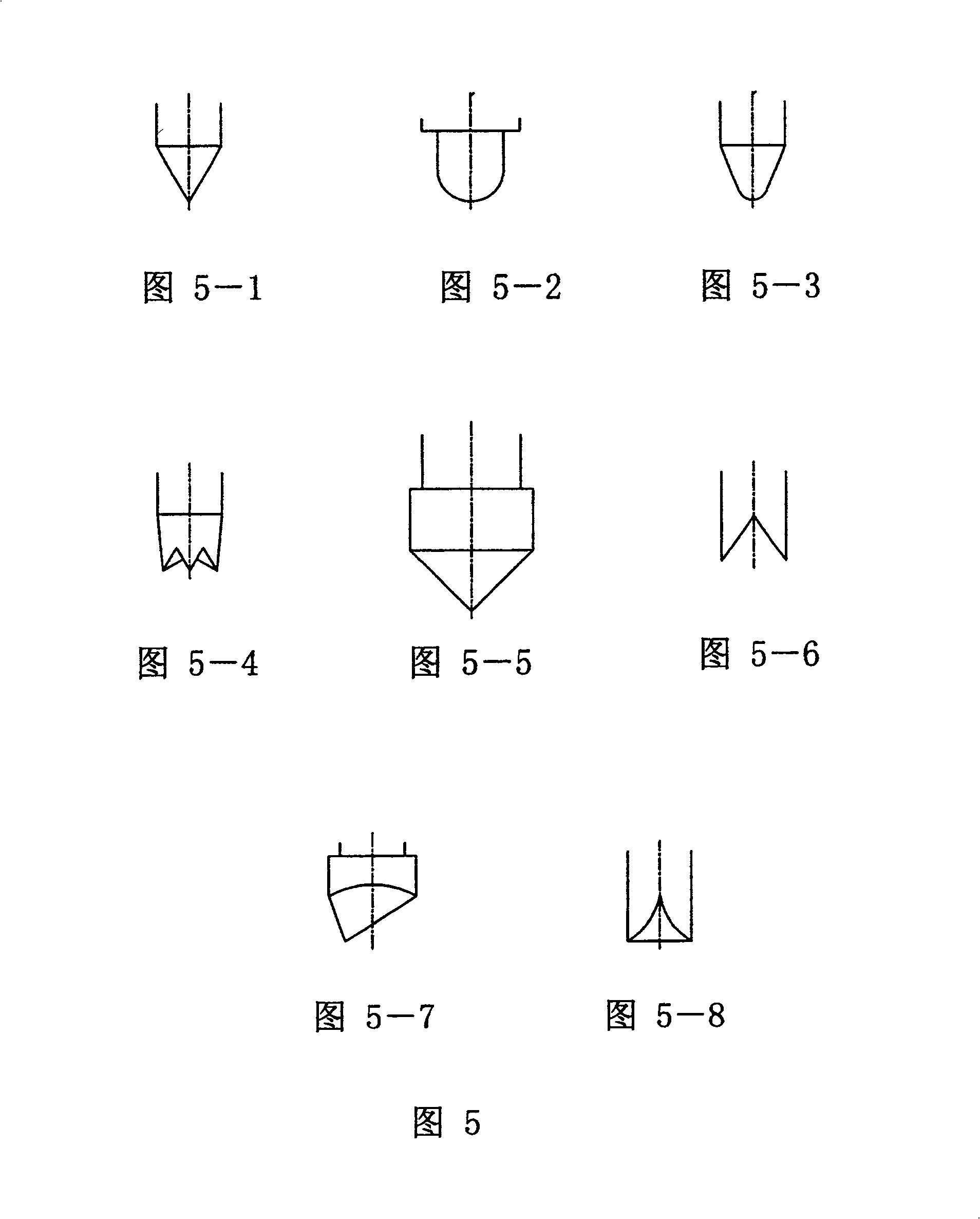
[0024] The combined probe for integrated circuit testing of the present invention, as shown in FIG. 1 , includes a single-headed probe 1 and a terminal 2 . another example Figure 10 As shown, the single-headed probe 1 is a commercially available single-headed probe with uniform specifications, including a head 13 and a tail body 12. The inner cavity of the body 12 is equipped with a spring, and the head 13 is inserted into the body 12. The inner cavity can move axially relative to the tube body 12; the top end of the head 13 has a head shape, and the end of the tail tube body 12 has a spring without a head shape, and the processing cost is extremely low. The head shape of the tip 11 of the single-headed probe 1 may be various shapes as shown in FIG. 5 . 2 to 4 , the upper part of the terminal 2 is hollow, the inner wall is provided with a clamping part, and eithe...


PUM


Abstract

The invention relates to a combination probes for testing integrated circuit, which comprises: single head probe (1) and terminal (2); the single head probe (1) includes head (13) and end tube (12) which has a spring in the cavity, the head (13) being inserted in the tube (12) inner cavity and moving relative to the tube (12); the upper part of the terminal (2) is hollow and a clamping part is provided in it, any end of the single head (1) being inserted into terminal (2) and its end part being clamped tightly by clamp; the other end of the single head probe (1), which is not inserted into the terminal (2), being electronic connected with the integrated circuit or circuit board for testing, correspondingly, the end (21) of the terminal (2) being employed for testing electronic connections of the testing circuit board or the integrated circuit. Compared with prior technology, the invention has the advantages of having low resistance, capacity reactance or inductive reactance.

Description

technical field [0001] The present invention relates to electrical performance testing or fault detection components of semiconductor devices, in particular to probes for testing integrated circuits. Background technique [0002] With the development of SMT, that is Surface Mount Technology, the semiconductor integrated circuit (hereinafter referred to as IC) especially adopts the Ball Grid Array Ball Grid Array referred to as BGA, that is, the arrangement of the input / output pins after packaging is a grid array . ICs with solder balls at the end of the pins are developing in the direction of high density and small spacing. The input / output pins of the package have gradually increased from dozens to hundreds, and may reach 2,000 in the near future. Therefore, the requirements for integrated circuit testing are getting higher and higher. There are two kinds of probes that can meet the IC testing requirements of high density and small spacing in the prior art, one such as F...

Claims


Application Information

Patent Timeline
Patent Type & Authority Patents(China)
IPC IPC(8): G01R1/067G01R1/02G01R31/26G01R31/28H01L21/66
Inventor 段超毅
Owner 武汉精毅通电子技术有限公司
Why Eureka
Try Eureka