

TFT LCD structure and producing method
A reflective electrode and substrate technology, applied in semiconductor/solid-state device manufacturing, photolithography process exposure devices, optics, etc., can solve the problems of low contrast, unsatisfactory display effect, unusable use, etc. The effect of low consumption and low energy consumption
- Summary
- Abstract
- Description
- Claims
- Application Information
AI Technical Summary
Problems solved by technology
Method used
Image

Examples
Embodiment 1
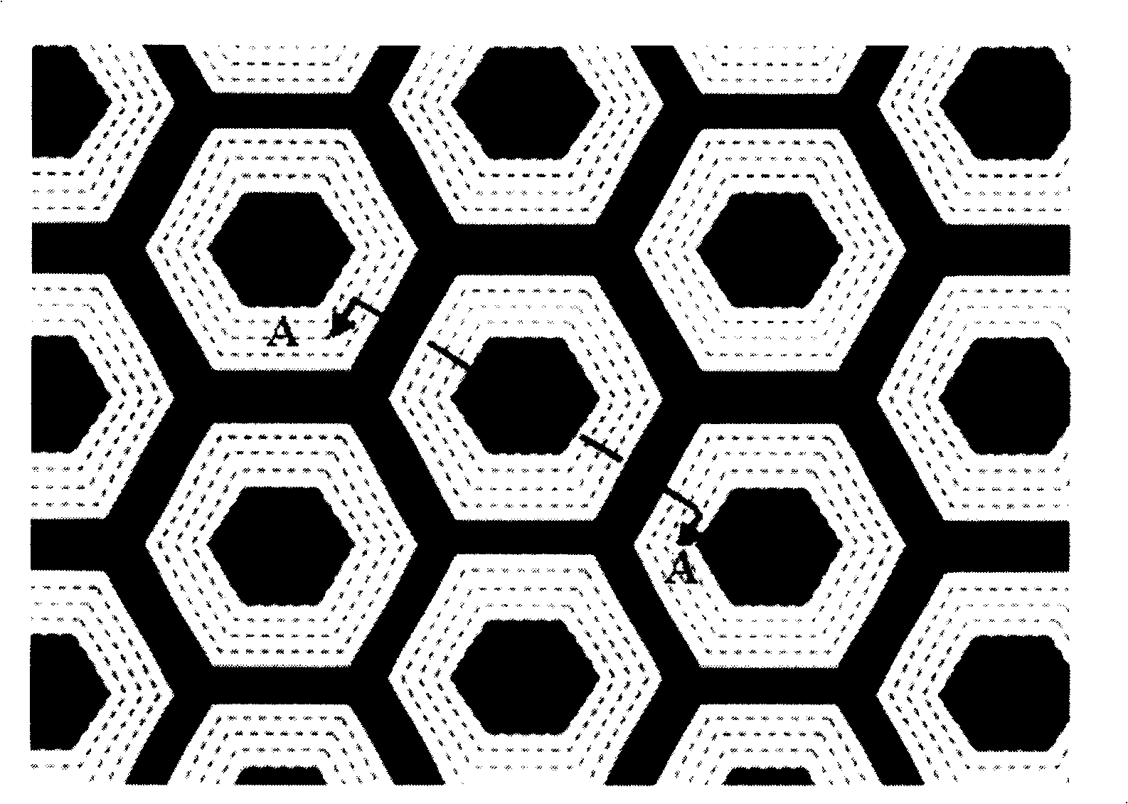
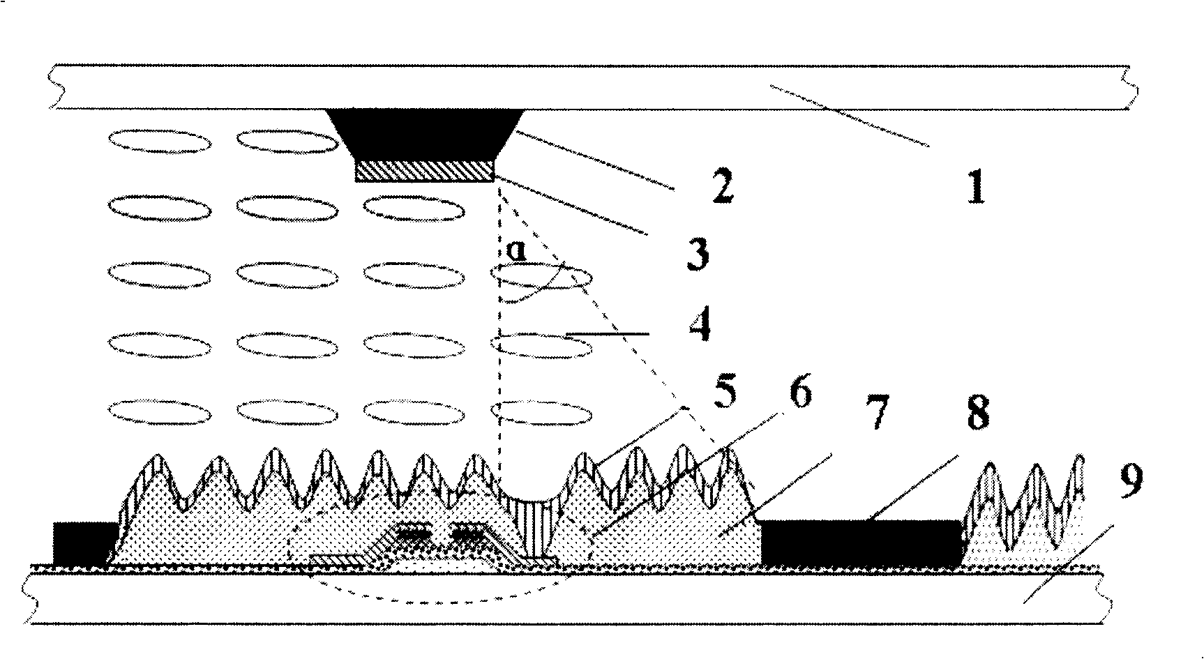
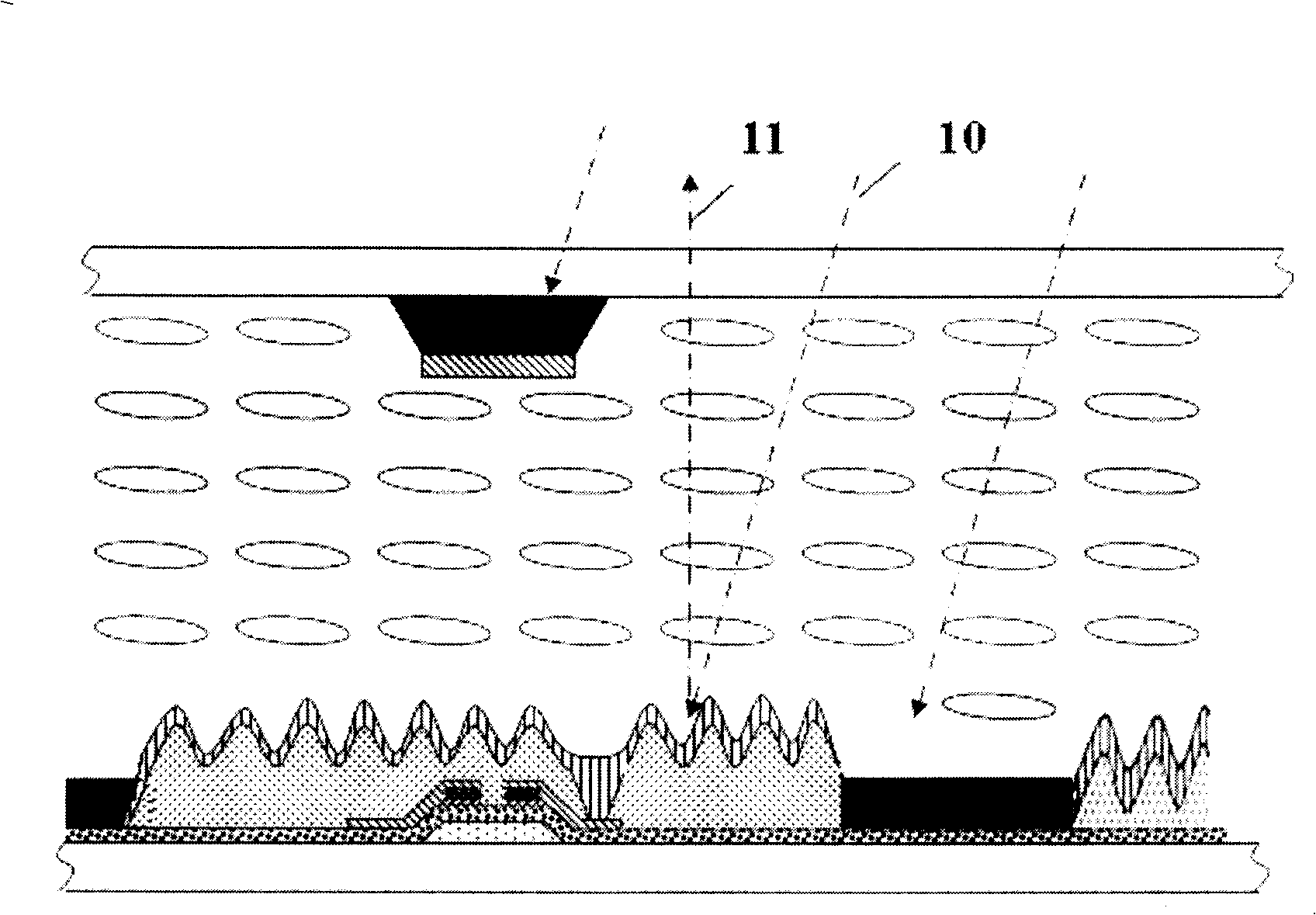
[0057] The concrete structure of an embodiment of the present invention is as figure 1 , figure 2 shown. In the embodiment, the main structure of the present invention has two layers of substrates: the upper substrate includes an upper insulating substrate 1; an upper light absorbing layer 2 is formed on the upper insulating substrate 1; a hexagonal upper reflective electrode The layer 3 is formed on the upper light absorbing layer 2, and the upper reflective electrode layers 3 are laterally connected by connecting wires.
[0058] The lower substrate includes a lower insulating substrate 9; gate lines and data lines formed on the lower insulating substrate 9, adjacent gate lines and data lines intersect to define a pixel area, each pixel area includes a thin film transistor 6; the cross section is positive The hexagonal concentric corrugated resin layer 7 covers the entire thin film transistor 6; the hexagonal lower reflective electrode layer 5 is formed on the resin layer ...
Embodiment 2
[0074] The specific structure of another embodiment of the present invention also includes: an upper substrate and a lower substrate, the liquid crystal layer is encapsulated between the upper substrate and the upper substrate, and the characteristics of the upper substrate are the same as those in Embodiment 1. The difference between this embodiment and embodiment 1 lies in the lower substrate, the specific structure of the lower substrate is as follows Figure 20 as shown in Figure 20As shown, the lower substrate includes: a lower insulating substrate; gate lines and data lines formed on the lower insulating substrate; adjacent gate lines and data lines intersect to define a pixel area, and each pixel area includes a thin film transistor; a section is A wavy hexagonal resin layer covering the entire thin film transistor device; these parts are the same as those in Embodiment 1, the difference being that: the lower light absorbing layer 8 is formed above the thin film transi...
PUM
 Abstract
Description
Claims
Application Information