

Method for reducing feature size and semi-conductor etching method
A feature size, semiconductor technology, applied in semiconductor/solid-state device manufacturing, electrical components, circuits, etc., can solve problems such as linear distortion, unstable photoresist, insufficient thickness of photoresist layer, etc., to achieve accurate effect of size
- Summary
- Abstract
- Description
- Claims
- Application Information
AI Technical Summary
Problems solved by technology
Method used
Image

Examples
Embodiment Construction
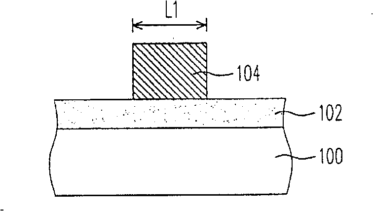
[0036] Figure 2A to Figure 2B Shown is a cross-sectional view of the fabrication process of a method for reducing feature size according to a preferred embodiment of the present invention. Please refer to Figure 2A Firstly, a dielectric layer 202 is formed on a substrate 200 . Wherein, the material of the dielectric layer is, for example, silicon oxide, silicon nitride or silicon oxynitride. A patterned photoresist layer 204 is then formed on the dielectric layer 202 to expose part of the dielectric layer 202 . Wherein, the patterned photoresist layer 204 has a first line width L1.
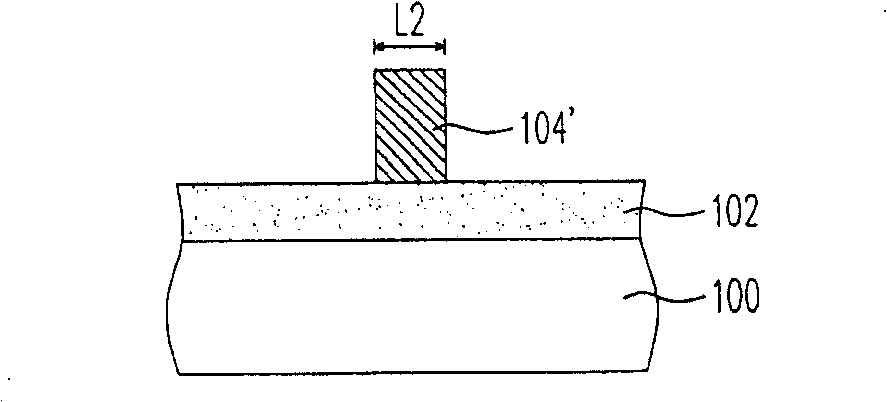
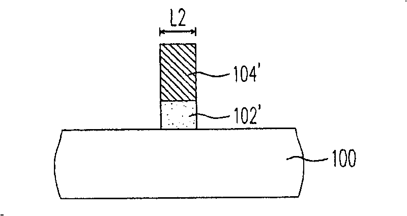
[0037] Next, please refer to Figure 2B , using the patterned photoresist layer 204 as an etching mask, an etching process is performed under an environment with a pressure of, for example, 80-400 Torr and a temperature of, for example, -50° C. to 50° C. to remove the exposed dielectric layer 202 and make the final line width L2 of the reduced patterned photoresist layer 204' and the patter...
PUM
 Abstract
Description
Claims
Application Information