a photolithography method

A technology of photolithography and photolithography pattern, which is applied in the field of photolithography, can solve the problem of photoresist drop and achieve the effect of improving the line width rough phenomenon

Active Publication Date: 2016-04-13
SEMICON MFG INT (SHANGHAI) CORP
View PDF4 Cites 0 Cited by
  • Summary
  • Abstract
  • Description
  • Claims
  • Application Information

AI Technical Summary

Problems solved by technology

[0004] In semiconductor manufacturing, resolution and sensitivity are also important parameters in photolithography steps. On the one hand, it is hoped to improve the resolution of photolithography, and on the other hand, it is also necessary to avoid the decline of photoresist sensitivity. From the calculation of RLS constant The relationship between the resolution, LWR and sensitivity expressed by the formula shows that in order to improve LWR, it is necessary to reduce the resolution and / or sensitivity in the photolithography process. Therefore, improving LWR and maintaining photoresist resolution The contradiction between rate and sensitivity has not been resolved

Method used


Image

  • a photolithography method
  • a photolithography method
  • a photolithography method

Examples


specific Embodiment 1

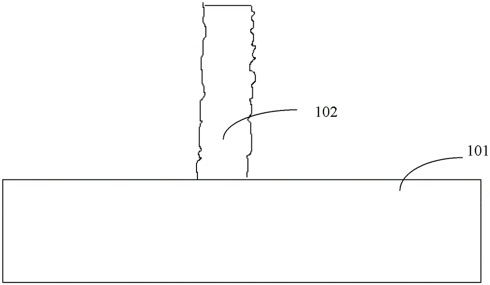
[0024] The photolithography method proposed by the present invention can effectively improve the line width roughness (LWR) phenomenon of the photolithographic pattern without reducing the resolution and sensitivity of the photoresist, thereby better controlling the etching of the dielectric layer to form a semiconductor Device CD.

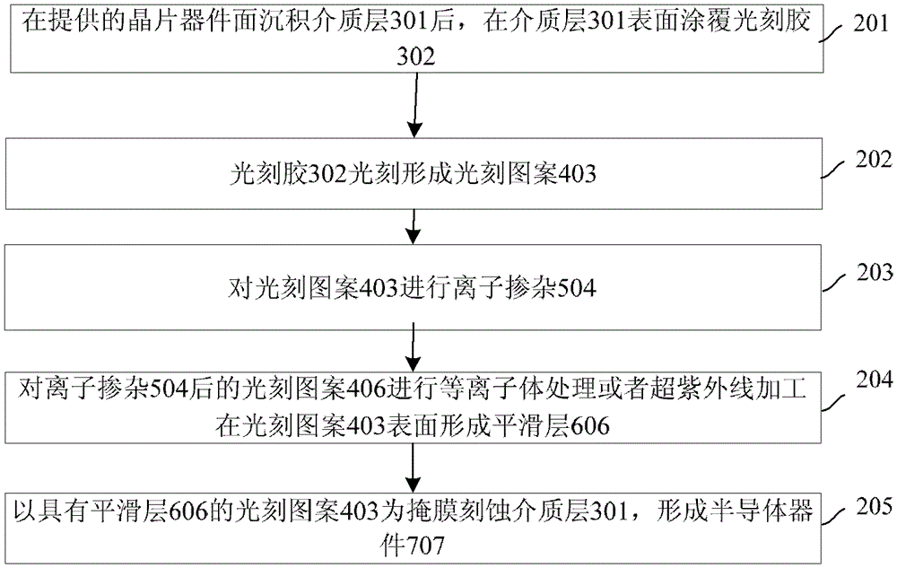
[0025] Combine below Figure 3-7 The simplified cross-sectional schematic diagram of the structure of the photolithography and etching method proposed by the present invention is shown in detail as figure 2 The flow chart of the photolithography and etching method steps proposed by the present invention is shown.

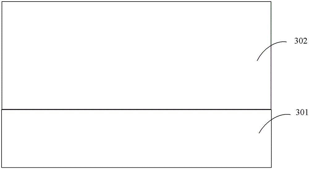
[0026] Step 201, image 3 A schematic diagram of the cross-sectional structure of step 201 of the etching method proposed by the present invention, such as image 3 As shown, after the dielectric layer 301 is deposited on the device surface of the provided wafer, a photoresist 302 is coated on the surface of the dielectric layer 301...


PUM

PropertyMeasurementUnit
wavelengthaaaaaaaaaa
thicknessaaaaaaaaaa

Abstract

The invention provides a lithography method. The method is characterized by carrying out lithography on a depositional dielectric layer so as to form a photoetching pattern; after that, doping is performed on the photoetching pattern and then plasma processing or extreme ultraviolet processing is performed; forming a smoothing layer on a surface of the photoetching pattern. Therefore, under the conditions that a photoresist resolution and a sensitivity are not reduced, a line-width rough phenomenon of the photoetching pattern is improved. A feature size of a semiconductor device is controlled, wherein the semiconductor device is formed by the dielectric layer which is etched by a mask layer; the photoetching pattern possessing the smoothing layer is taken as the mask layer.

Description

technical field [0001] The invention relates to a semiconductor manufacturing method, in particular to a photolithography method. Background technique [0002] With the advancement of semiconductor manufacturing technology, while the size of semiconductor devices is continuously shrinking, the feature size (CD) of semiconductor devices is also required to be smaller and smaller. As we all know, the process flow of semiconductor manufacturing technology includes two very important steps: photolithography and etching; among them, the etching step often uses the photolithography pattern formed in the photolithography step as a mask to transfer the photolithography pattern to On the wafer, the photolithography process, which plays an important role in CD control, has been challenged unprecedentedly. The distance between the edges of the photolithographic pattern formed after lithography is called the line width (LineWidth). An important indicator to measure the line width is th...

Claims


Application Information

Patent Timeline
Patent Type & Authority Patents(China)
IPC IPC(8): H01L21/027G03F7/00G03F7/20
Inventor 沈满华
Owner SEMICON MFG INT (SHANGHAI) CORP
Why Eureka
Try Eureka