Semiconductor device and forming method thereof

A semiconductor and device technology, applied in the field of semiconductor devices and their formation, can solve problems such as poor performance of semiconductor devices

Active Publication Date: 2019-03-01
SEMICON MFG INT (SHANGHAI) CORP +1
View PDF17 Cites 0 Cited by
  • Summary
  • Abstract
  • Description
  • Claims
  • Application Information

AI Technical Summary

Problems solved by technology

[0004] However, the performance of the semiconductor device formed by the interconnection structure formed by the prior art is poor

Method used


Image

  • Semiconductor device and forming method thereof
  • Semiconductor device and forming method thereof
  • Semiconductor device and forming method thereof

Examples


Embodiment Construction

[0030] As mentioned in the background, semiconductor devices formed in the prior art have poor performance.

[0031] Figure 1 to Figure 3 It is a structural schematic diagram of the formation process of a semiconductor device.

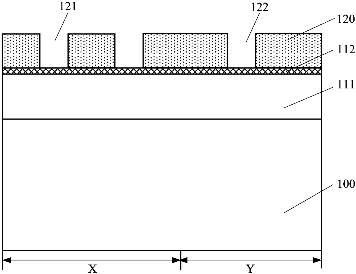
[0032] refer to figure 1 , provide the layer to be etched 100, the layer to be etched 100 includes a sparse area Y and a dense area X, the layer to be etched 100 has a flat layer 111, a bottom anti-reflective layer 112 on the flat layer 111, and a bottom antireflective layer on the bottom The photoresist layer 120 on the surface of the antireflection layer 112, the photoresist layer 120 has a first mask opening 121 and a second mask opening 122 penetrating through the photoresist layer 120, the first mask opening 121 is located on the dense area, The second mask opening 122 is located on the sparse area Y.

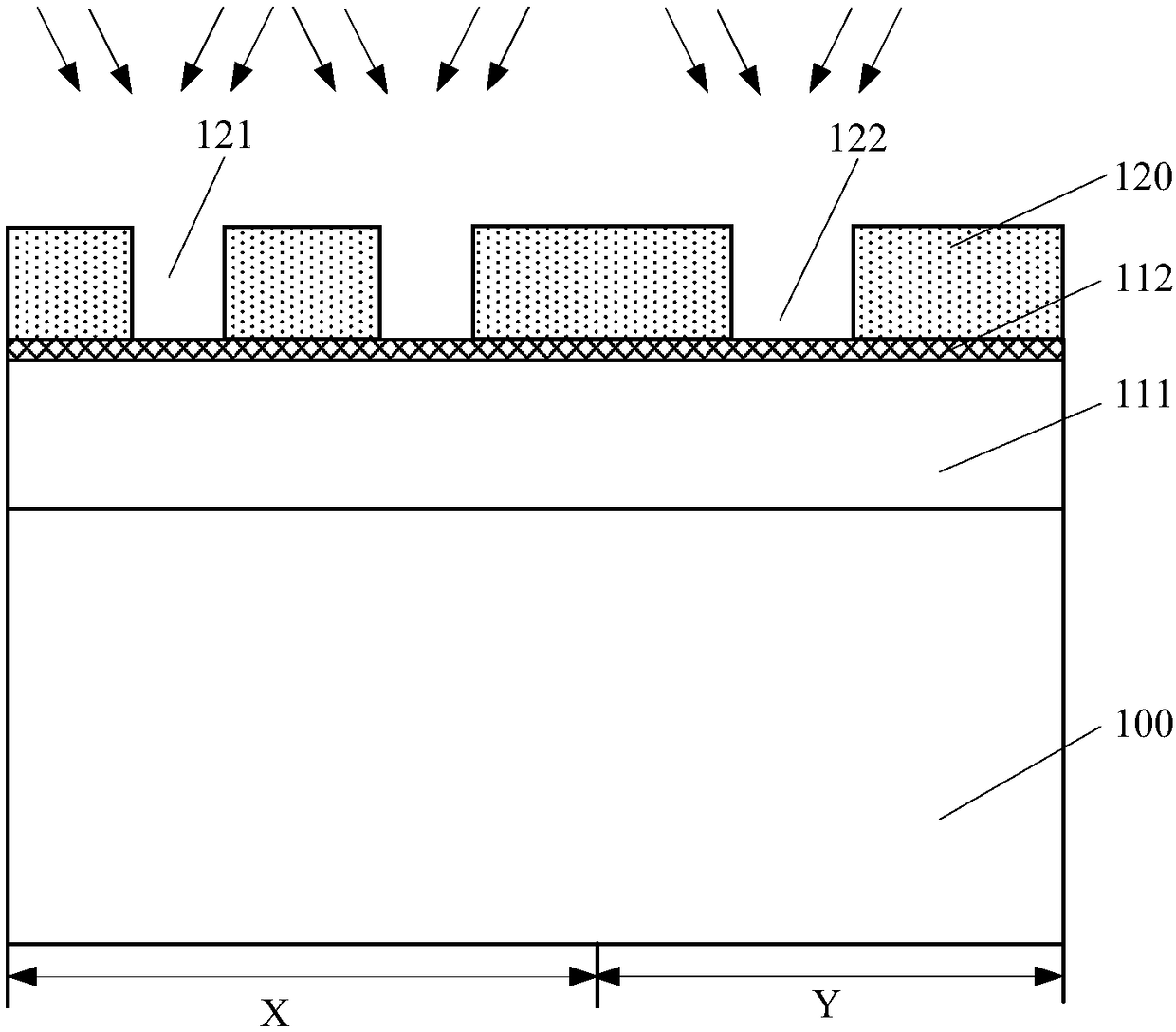
[0033] refer to figure 2, carry out plasma treatment to the photoresist layer 120 side wall, the gas that plasma treatment adopts comprises ...


PUM


Abstract

The invention provides a semiconductor device and a forming method thereof. The method comprises the following steps: performing plasma processing on a side wall of a photoresist layer, wherein bottomanti-reflection layers at the bottoms of a first opening and a second opening are also etched by the plasma processing craft, the surfaces of the bottom anti-reflection layers are concave, and the concave degree of the surface of the bottom anti-reflective layer at the bottom of the second opening is greater than that of the surface of the bottom anti-reflective layer at the bottom of the first opening; then etching the bottom anti-reflective layers at the bottoms of the first opening and the second opening to correspondingly form a third opening and a fourth opening, which pass through the bottom anti-reflective layers in the bottom anti-reflective layers at the bottoms of the first opening and the second opening, wherein the bottom width of the fourth opening is smaller than the bottomwidth of the third opening; and etching a layer to be etched at the bottom of the third opening and the layer to be etched at the bottom of the fourth opening to form first grooves in dense areas of the layers to be etched and to form second grooves in sparse areas of the layers to be etched. The performance of the semiconductor device is improved.

Description

technical field [0001] The invention relates to the field of semiconductor manufacturing, in particular to a semiconductor device and a forming method thereof. Background technique [0002] With the continuous advancement of semiconductor integrated circuit process technology, when semiconductor devices are reduced to a deep submicron range, high-performance, high-density connections between semiconductor devices need to be realized through interconnect structures. [0003] Based on the requirements of integrated circuit design, the interconnection structure has a sparse area and a dense area, and the density of the interconnection structure in the dense area is greater than the density of the interconnection structure in the sparse area. Generally, the interconnection structure in the dense area and the interconnection structure in the sparse area are formed in the same process. [0004] However, the performance of the semiconductor device formed by the interconnection str...

Claims


Application Information

Patent Timeline
Patent Type & Authority Applications(China)
IPC IPC(8): H01L21/027H01L21/266H01L21/3065
CPCH01L21/0273H01L21/0276H01L21/266H01L21/3065
Inventor 张城龙刘盼盼郑二虎
Owner SEMICON MFG INT (SHANGHAI) CORP
Why Eureka
Try Eureka