Organic electroluminescence display of black electrode structure and its manufacturing method

A technology of electrode structure and manufacturing method, which is applied in the fields of electrical solid-state devices, semiconductor/solid-state device manufacturing, circuits, etc., can solve the problems of unfavorable mass production of OLED devices, etc., and achieve the effects of prolonging the production takt time, matching well, and improving contrast

Active Publication Date: 2009-06-03
TRULY SEMICON
View PDF6 Cites 0 Cited by
  • Summary
  • Abstract
  • Description
  • Claims
  • Application Information

AI Technical Summary

Problems solved by technology

However, the sputtering method has a great negative impact on thin-layer metal electrodes, electron transport layers and electron injection layers, which is not conducive to the mass production of OLED devices. Therefore, the literature also mentions the use of evaporation methods to evaporate organic materials instead of Inorganic materials, such as the co-evaporation method of organic materials and metals mentioned in Applied Physics Letters 83 (2003) 186-189
However, in the prior art, only one organic or inorganic material is used for the functional layer between the thin-layer metal electrode and the reflective metal electrode, and the black electrode is made by using the principle of destructive interference of light. However, it is impossible for one material to be used in the entire There are light absorption characteristics in the visible spectrum, and its refractive index is also fixed, so there are great limitations in optimizing the reflectivity of the black electrode and the color coordinates of the reflection spectrum

Method used


Image

  • Organic electroluminescence display of black electrode structure and its manufacturing method
  • Organic electroluminescence display of black electrode structure and its manufacturing method
  • Organic electroluminescence display of black electrode structure and its manufacturing method

Examples


Embodiment 1

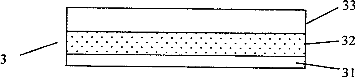
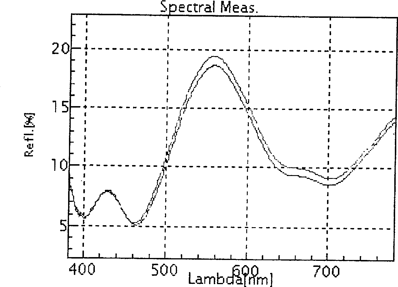
[0027] Embodiment 1, the thin metal electrode reflective layer 31 adopts an aluminum material with a thickness of 3 nanometers, and the organic material functional layer 32 selects CuPc that absorbs red light and Alq3 that absorbs UV-blue light, and its thickness is 70 nanometers. The ratio of the two materials is 1:1, image 3 It is the reflectance spectrum curve diagram of the blue light device adopting the above embodiment.

Embodiment 2

[0028] Embodiment 2. The thin metal electrode reflective layer 31 is made of an aluminum material with a thickness of 3.5 nanometers, and the organic material functional layer 32 is made of CuPc and Rubrene with a thickness of 70 nanometers, and the ratio of the two materials is 1:1. , Figure 4 It is the reflectance spectrum curve diagram of the blue light device adopting the above embodiment.

Embodiment 3

[0029] Embodiment 3. The thin metal electrode reflective layer 31 is made of an aluminum material with a thickness of 4 nanometers, and the organic material functional layer 32 is made of CuPc and Rubrene with a thickness of 90 nanometers. Figure 5 The reflectance spectrum curves of the blue light device when the ratio of the above two materials are 90:0, 80:10 and 70:20 are listed in . The reflectivity of the device whose black electrode is mixed with the above two materials is significantly lower than that of the ordinary device, and is also lower than that of the device whose black electrode is only made of one material (CuPc:Rubrene=90:0).

[0030] The organic electroluminescent display with black electrode structure of the present invention is produced by vacuum evaporation using high vacuum coating equipment, and the entire production process is completed at one time without breaking the vacuum. All the following steps:

[0031] A. Clean the anode substrate;

[0032] B...


PUM


Abstract

An organic electroluminescent display with black electrode structure is prepared as setting a luminous layer on organic film layer, utilizing cathode as black electrode formed by thin metal electrode reflection layer and organic material functional layer as well as thick metal electrode reflection layer, forming organic material functional layer by at least two types of organic materials being used to complement optical property to each other so as to decrease light reflectivity of visible light. The preparing method of black electrode is also disclosed.

Description

technical field [0001] The invention relates to an organic electroluminescent display and a manufacturing method thereof, in particular to an organic electroluminescent display with a black electrode structure and a manufacturing method thereof. Background technique [0002] Since Deng Qingyun of Kodak Company first developed a low driving voltage (<10V, >1000cd / m2) OLED device (Alq3 as the light-emitting layer) with practical value for the first time in 1987, OLED technology is gradually being put into practical use, and organic light-emitting displays are considered to be The new generation of flat light-emitting displays will face a new revolution in display technology. Because it has many advantages such as active light emission, high contrast ratio, thinness, and fast response speed, it is recognized as the main force of the next-generation display. However, due to the relatively high reflectivity of the aluminum and magnesium-silver cathode electrodes, the contr...

Claims


Application Information

Patent Timeline
Patent Type & Authority Patents(China)
IPC IPC(8): H01L51/50H01L51/54H01L51/56H01L27/32
Inventor 路林邝颂贤
Owner TRULY SEMICON
Why Eureka
Try Eureka