Data by-passage technology in digital signal processor
A digital signal, bypass system technology, applied in machine execution devices, concurrent instruction execution, etc., can solve the problems of not getting results, stalling and waiting, and achieve the effects of reducing conflict stalls, increasing clocks, and reducing delays
- Summary
- Abstract
- Description
- Claims
- Application Information
AI Technical Summary
Problems solved by technology
Method used
Image
Examples
example 1
[0061] Example 1, consider the following 2 instructions:
[0062] ADD A, B, C
[0063] SUB D, A, E
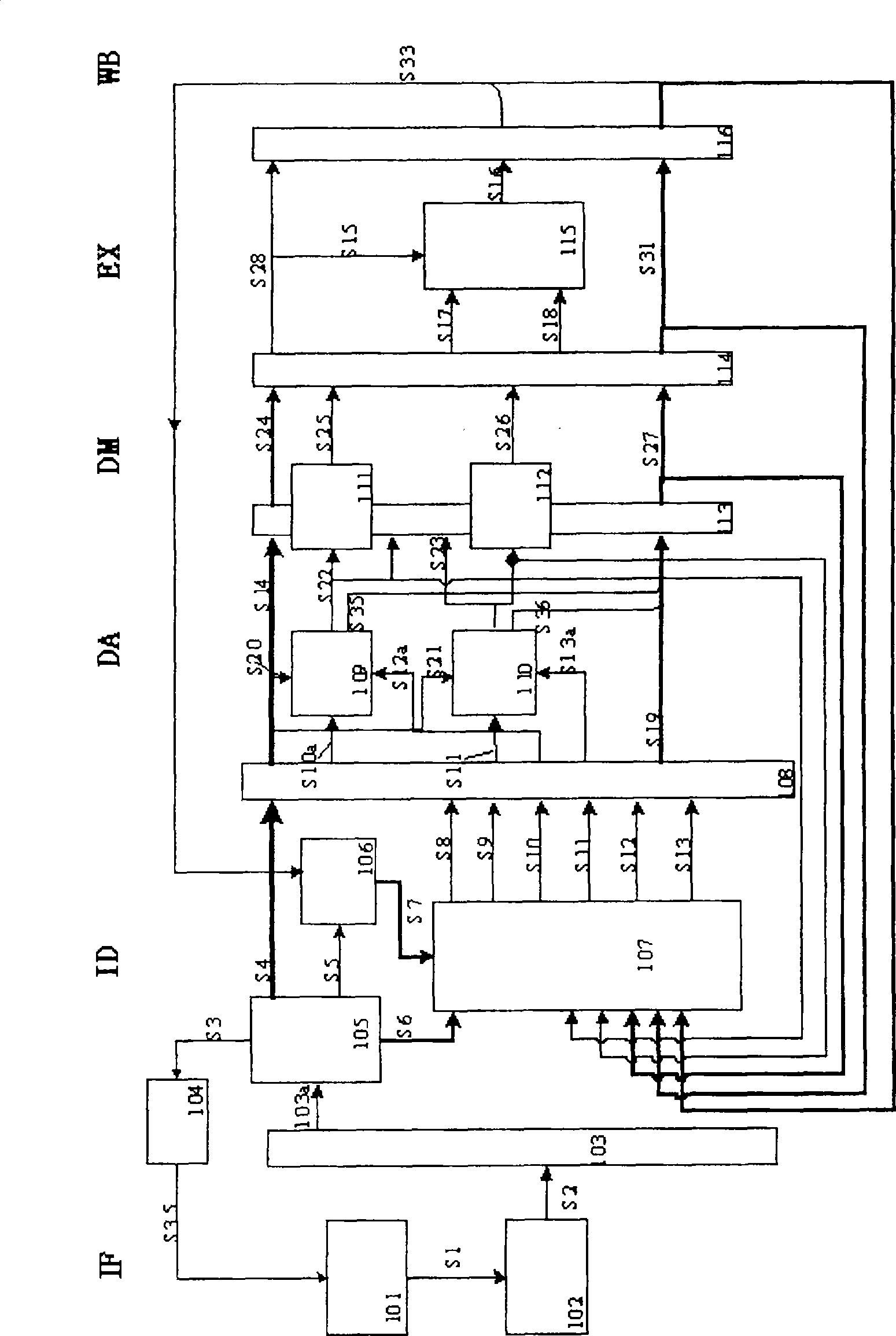
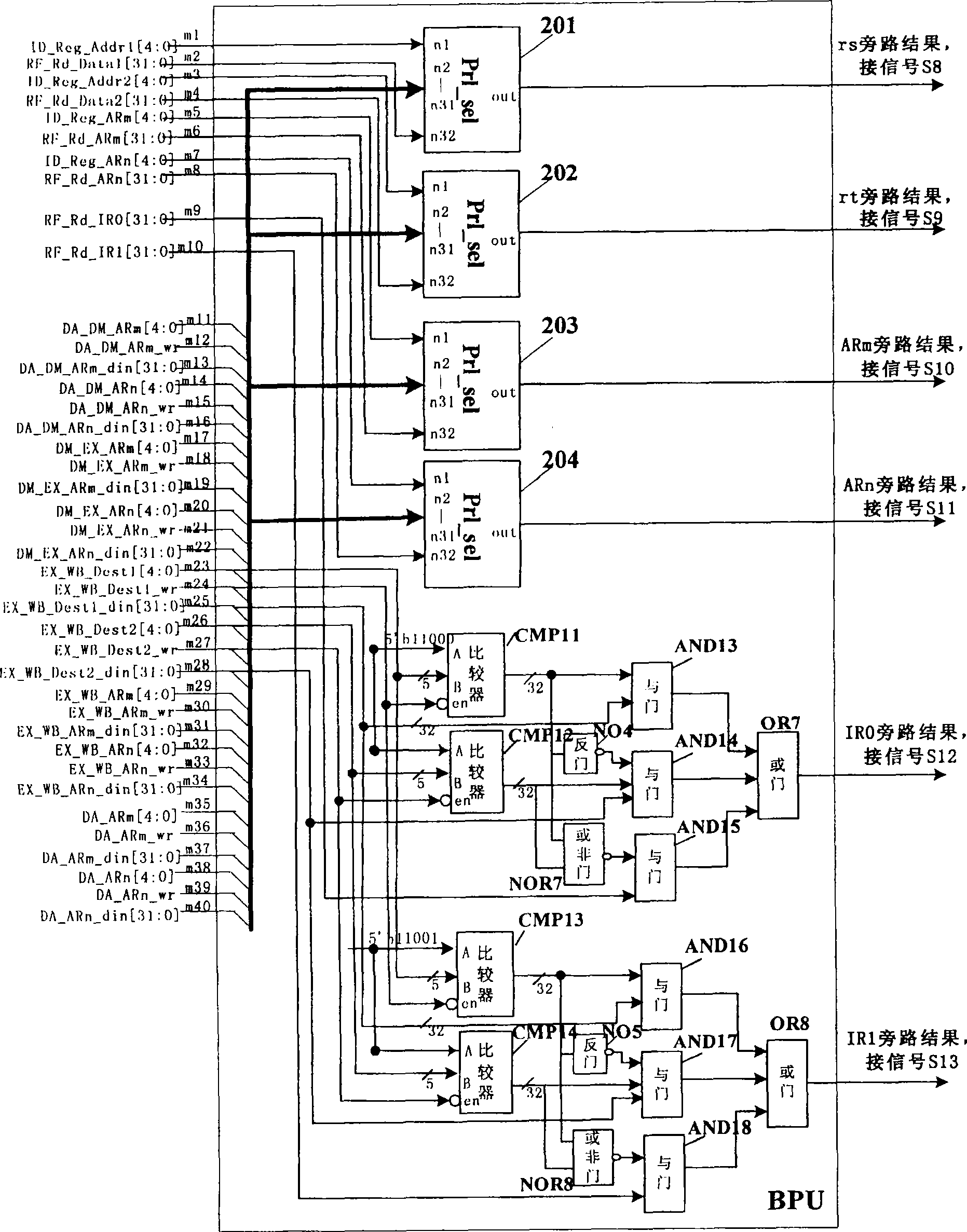
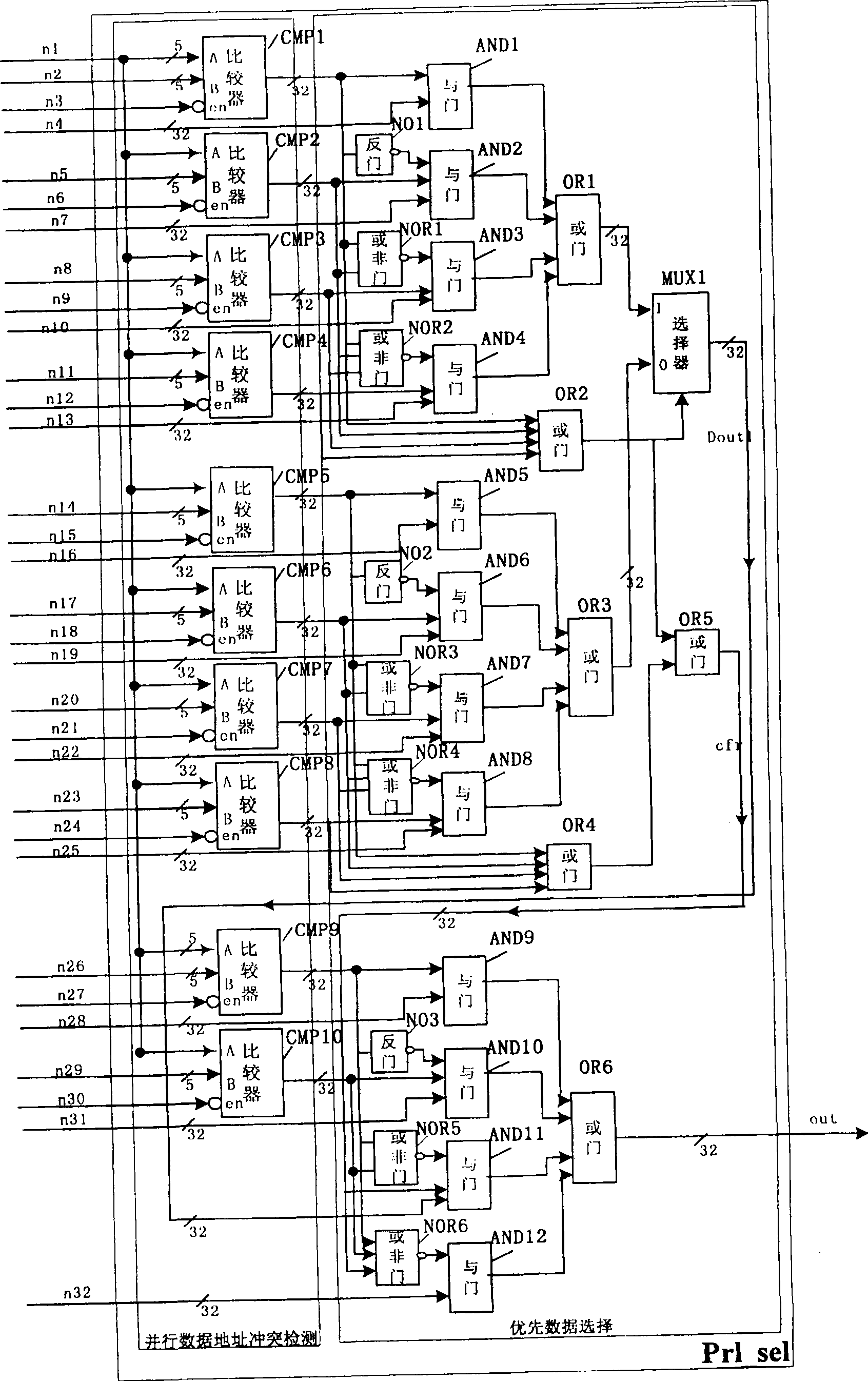
[0064] The first instruction performs the operation of B+C and stores the result in register A. The second instruction performs the A-E operation and stores the result in register D. Since the source register A of the second instruction uses the calculation result of the first instruction, there is a data dependency between the two instructions. Therefore, when the second instruction is at the decoding stage, the control unit will judge the data conflict control information S35, so that the pipeline IF and ID will stop, while other stages continue to execute. Until the first instruction is executed to the WB level, the parallel data conflict detection in the data bypass circuit compares the address value, the comparator CMP5 will find that the read address and the write address are the same, both are A registers, and the output cc5 of the comparator CMP5 will change to Comp...
example 2
[0065] Example 2, consider the following 3 instructions:
[0066] ADD ARm, B, C
[0067] SUB D, *ARm++(IR0), *ARn++(IR1)
[0068] ADD E, *ARm+(4), F
[0069] The first instruction is an addition instruction, which realizes B+C, and the result is stored in the address register ARm. The second instruction is more complicated, and it implements a subtraction operation. The two operands come from the memory numbers whose addresses are ARm+IR0 and ARn+IR1. At the same time, the value of the ARm register will be updated to the value of ARm+IR0, and the value of the ARn register will be updated to the value of ARn+IR1. The result of the subtraction is stored in register D. The third instruction is still an addition instruction. The two operands come from the memory number, the memory address is the result of ARm+4, and the other operand comes from the register F. In this example, there is a data correlation between the ARm of the first instruction and the second instruction, and...
PUM
 Abstract
Description
Claims
Application Information


