

Flat-board display of hollow bottom grid array structure and mfg. technology
A flat panel display and array structure technology, applied in the field of flat panel display technology, can solve the problems of large gate current and high operating voltage.
- Summary
- Abstract
- Description
- Claims
- Application Information
AI Technical Summary
Problems solved by technology
Method used
Image

Examples
Embodiment Construction
[0035] The present invention will be further described below in conjunction with the accompanying drawings and embodiments, but the present invention is not limited to these embodiments.
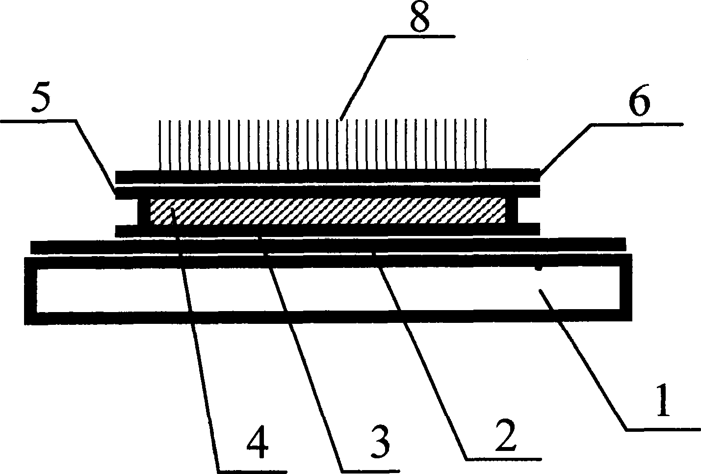
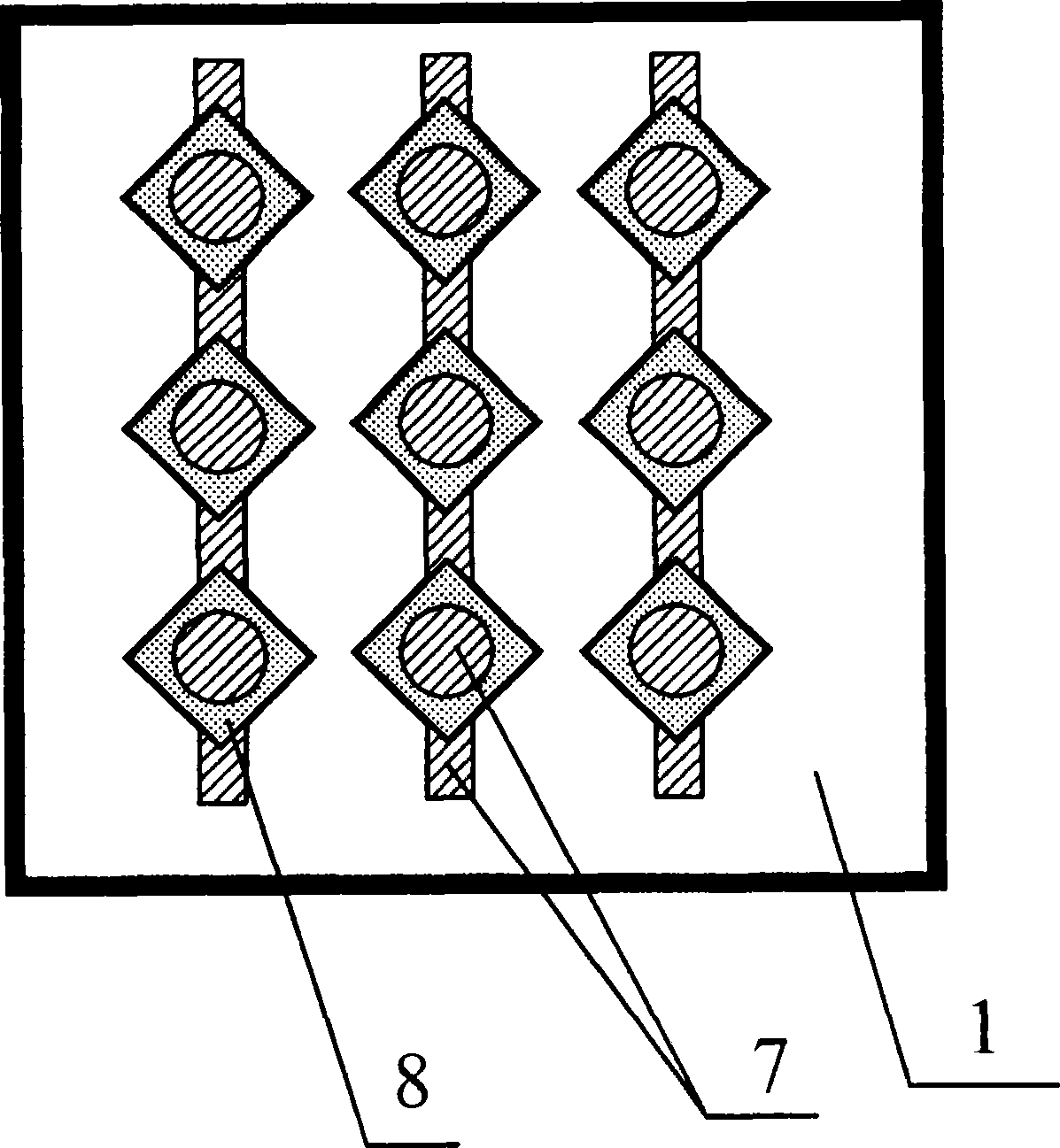
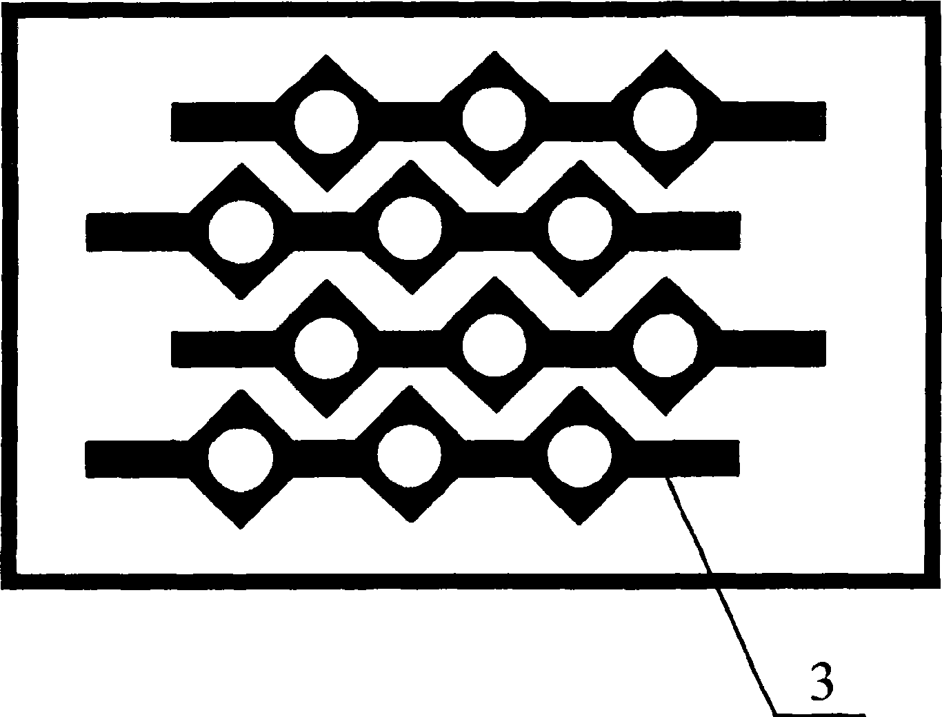
[0036] Described a kind of flat panel display with hollow bottom grid array structure, comprises the airtight vacuum cavity that is made of cathode glass panel 1, anode glass panel 9 and surrounding glass frame 15; An anode conductive layer 10 is arranged on the anode glass panel , preparing the phosphor layer 12 on the anode conductive layer and printing the insulating paste layer 11 on the non-display area of the anode conductive layer; the support wall structure 14 between the anode glass panel and the cathode glass panel and the getter accessory element 13, There are cathode conductive layer 6, carbon nanotubes 8 and hollow bottom grid array structure on the cathode glass panel.
[0037] The substrate material of the hollow bottom grid array structure is glass, such as soda lime glass,...
PUM
 Abstract
Description
Claims
Application Information