Planar display device with H-shaped sided-grid controlled structure and its production

A flat-panel display and manufacturing process technology, applied in the direction of control electrodes, discharge tube/lamp manufacturing, image/graphic display tubes, etc., can solve problems such as large grid current and high grid voltage

A flat-panel display and manufacturing process technology, applied in the direction of control electrodes, discharge tube/lamp manufacturing, image/graphic display tubes, etc., can solve problems such as large grid current and high grid voltage

CN101075540AInactive Publication Date: 2007-11-21ZHONGYUAN ENGINEERING COLLEGE

Image

  • Planar display device with H-shaped sided-grid controlled structure and its production
  • Planar display device with H-shaped sided-grid controlled structure and its production
  • Planar display device with H-shaped sided-grid controlled structure and its production

Examples


Embodiment Construction

[0041] The present invention will be further described below in conjunction with the accompanying drawings and embodiments, but the present invention is not limited to these embodiments.

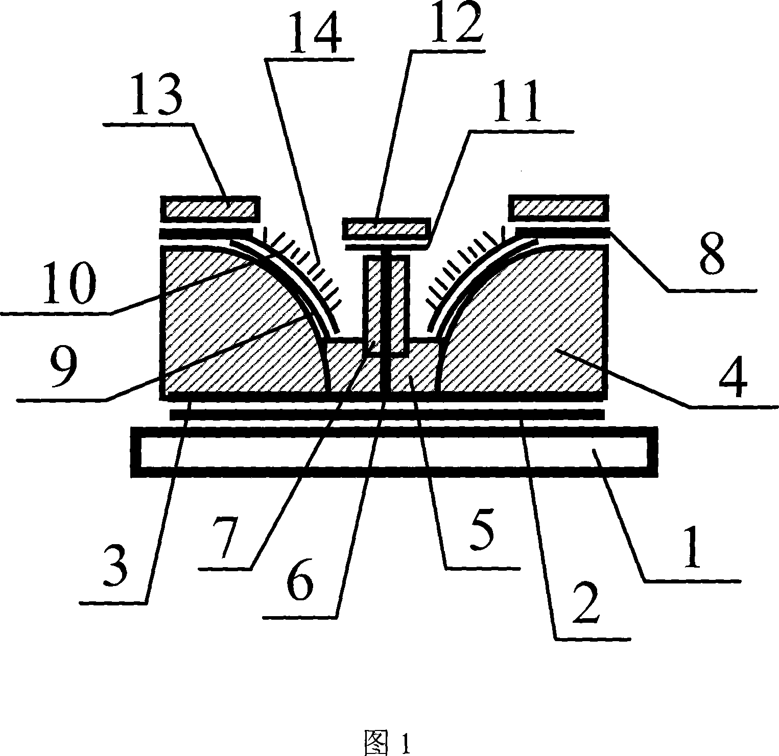
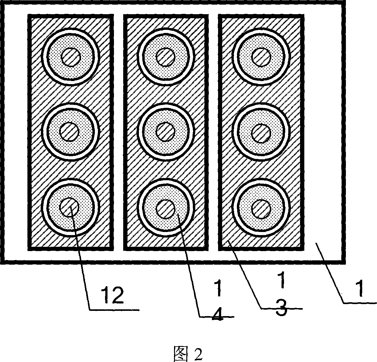
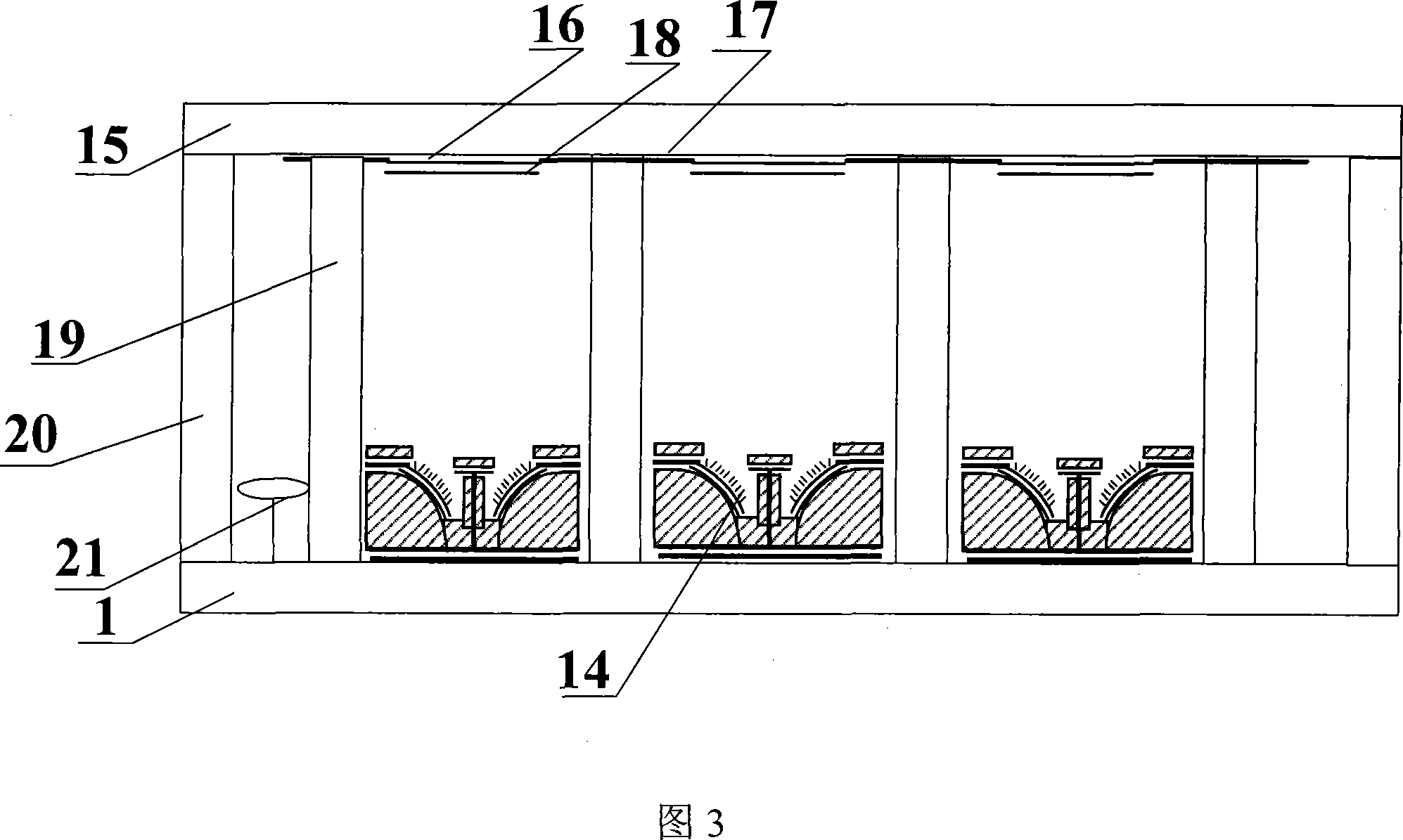
[0042] The present invention comprises a sealed vacuum chamber made of an anode glass panel [15], a cathode glass panel [1] and surrounding glass frames [20]; an anode conductive layer [16] is arranged on the anode glass panel and prepared on the anode conductive layer The upper phosphor layer [18]; there is a grid lead layer [3], carbon nanotubes [14] and I-shaped side grid control structure on the cathode glass panel; a support wall between the anode glass panel and the cathode glass panel Structure [19] and getter [21] accessory elements.

[0043] The I-shaped side gate control structure includes a cathode glass panel [1], a retardation layer [2], a grid lead layer [3], a cathode elevation layer [4], an isolation layer [5], and a grid extension line Layer [6], second isolation layer [7],...


PUM


Abstract

This is a flat displayer of I shape side grid cathode structure and its production process. It includes a sealed vacuum chamber formed by a anodic glass panel, a cathode glass panel and surrounded glass frame; on the anodic glass panel is a conducting layer coated with fluorescent; a supporting wall between the anodic and cathode panel and a getter; on the cathode glass panel are a grid down-lead layer, carbon nanotube and I shape side grid structure, which is capable of increasing the electron ejecting area and efficiency of the nanotube and increasing the control function of the grid.

Description

technical field [0001] The invention belongs to the fields of flat panel display technology, microelectronic science and technology, vacuum science and technology, and nano science and technology, and relates to device fabrication of flat panel field emission displays, in particular to carbon nanotube cathodes. The device manufacturing aspect of the flat panel field emission display particularly relates to a flat panel display with an I-shaped side gate control structure and its manufacturing process. Background technique [0002] Carbon nanotube cathode field emission display is a new type of flat panel display device, which makes full use of the cold field emission characteristics of carbon nanotubes, and uses the strength of an external electric field to force the tip of carbon nanotubes to emit electrons instead of using thermal energy to make field emission The energy distribution of the electron beam is narrow and has high brightness. The display is very thin, light, ...

Claims


Application Information

Patent Timeline
21 Nov 2007
Publication
CN101075540A
IPC
H01J31/12; H01J31/15; H01J29/02; H01J29/04; H01J1/304; H01J1/46; H01J9/02; H01J9/00
Inventors
李玉魁