Optical device, wave length variable filter, wave length variable filter module and spectral analysis device

A filter and variable technology, applied in the field of spectrum analyzer, can solve the problems of high driving voltage, difficult detection, large coupling capacitance, etc.

Inactive Publication Date: 2009-09-09
SEIKO EPSON CORP
View PDF5 Cites 2 Cited by
  • Summary
  • Abstract
  • Description
  • Claims
  • Application Information

AI Technical Summary

Problems solved by technology

[0006] However, in the variable wavelength filter of Patent Document 1, since the surface of the supporting substrate on the side of the movable part is a plane, the detection electrodes and the drive electrodes must be placed on the same plane. If the distance between the drive electrodes and the detection electrodes is small, , the coupling capacitance generated between them becomes large, making it difficult to correctly perform the detection
[0007] In addition, if the distance between the driving electrode and the detecting electrode is increased in order to reduce the coupling capacitance generated between the driving electrode and the detecting electrode, the area of ​​the driving electrode must be reduced for this reason, resulting in a lower driving voltage. Becomes high

Method used


Image

  • Optical device, wave length variable filter, wave length variable filter module and spectral analysis device
  • Optical device, wave length variable filter, wave length variable filter module and spectral analysis device
  • Optical device, wave length variable filter, wave length variable filter module and spectral analysis device

Examples


Embodiment Construction

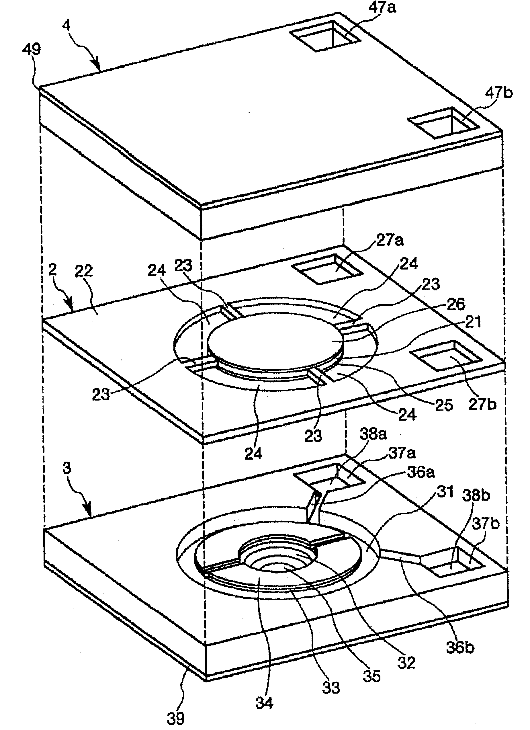
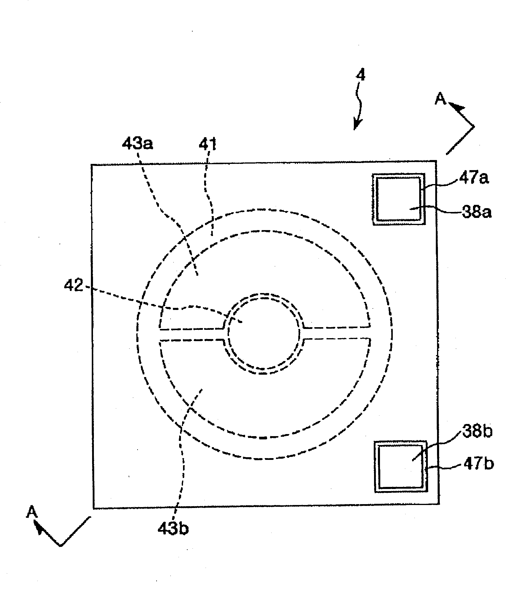
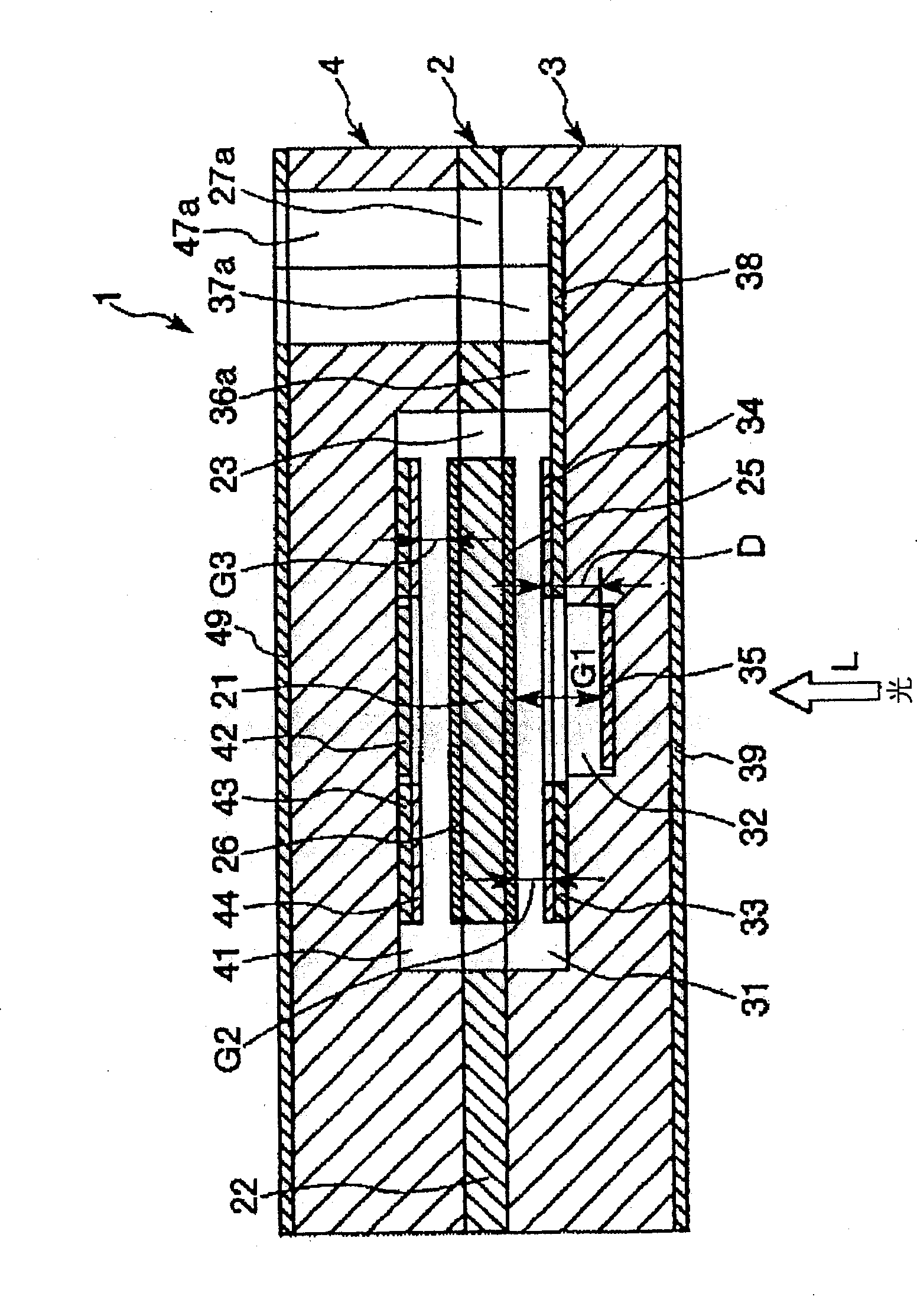
[0092] Hereinafter, the optical device, variable wavelength filter, variable wavelength filter module, and spectrum analyzer of the present invention will be described in detail based on preferred embodiments shown in the drawings.

[0093] figure 1 It is an exploded perspective view showing an embodiment of the optical device of the present invention, figure 2 yes figure 1 A top view of the optical device shown, image 3 yes figure 2 A-A line profile, Figure 4 is for illustration figure 1 The diagram of the drive electrode and detection electrode of the optical device shown, Figure 5 yes means figure 1 A block diagram showing the structure of the control system of the optical device. Also, in the description below, the figure 1 The upper side is "Up" and the lower side is "Down", figure 2 in and Figure 4 The front side of the paper in the paper is "Up", the inside of the paper is "Down", the right side is "Right", and the left side is "Left". image 3 The upp...


PUM

PropertyMeasurementUnit
thicknessaaaaaaaaaa

Abstract

An optical device includes a movable portion and a fixed portion having a first light reflection portion. The movable portion has a second light reflection portion facing the first light reflection portion with a first gap. The first and second light reflection portions are configured to reflect light repeatedly between the first and second light reflection portions so as to cause interference and emit light having a wavelength corresponding to a size of the first gap. The optical device also includes a first electrode portion fixed to the fixed portion so as to face a surface of the movable portion near the first light reflection portion with a second gap between the movable portion and the first electrode portion. The optical device has a second electrode portion fixed to the fixed portion so as to face another surface of the movable portion with a third gap between the movable portion and the second electrode portion. One of the first and second electrode portions serves as a detection electrode for detecting a capacitance between the movable portion and the detection electrode. Another of the first and second electrode portions serves as a drive electrode. The optical device includes a circuit operable to generate a potential difference between the movable portion and the drive electrode so as to generate an electrostatic attraction force therebetween for changing a position and / or a posture of the movable portion.

Description

technical field [0001] The invention relates to an optical device, a variable wavelength filter, a variable wavelength filter module and a spectrum analyzer. Background technique [0002] As an optical device, for example, a wavelength tunable filter (Optical Tunable Filter) for separating only light of a specific wavelength from light having a plurality of wavelengths is known (for example, refer to Patent Document 1). [0003] For example, the variable wavelength filter of Patent Document 1 is in the shape of a plate, and the movable part displaceable in the thickness direction thereof is arranged approximately parallel to the supporting substrate, and the surface of the movable part on the supporting substrate side is in contact with the supporting substrate. Reflective films are respectively provided on the surfaces (opposite surfaces) on the side of the movable part. [0004] Also, the driving electrodes are provided on the support substrate, and a potential difference...

Claims


Application Information

Patent Timeline
Patent Type & Authority Patents(China)
IPC IPC(8): G02B26/00G02B1/11B81B3/00G01J3/26G02B5/28
Inventor 中村亮介
Owner SEIKO EPSON CORP
Why Eureka
Try Eureka