Production method of high voltage MOS transistor

A technology of a MOS transistor and a manufacturing method is applied in the manufacture of high-voltage MOS transistors, the manufacture of high-voltage MOS transistors, and the field of preventing double-peak effects, which can solve the problems of reduced gate oxide threshold voltage, poor device stability, and high device power consumption. Effect of device power consumption, increased stability, and avoidance of double peaks

Inactive Publication Date: 2009-09-09
SEMICON MFG INT (SHANGHAI) CORP +1
View PDF4 Cites 0 Cited by
  • Summary
  • Abstract
  • Description
  • Claims
  • Application Information

AI Technical Summary

Problems solved by technology

[0010] The problem to be solved by the present invention is to provide a method for manufacturing a semiconductor transistor, which prevents gate oxidation from being easily caused during the formation of the gate oxide layer due to the fact that the gate oxide layer of the high-voltage MOS transistor is relatively thick and is affected by the chamfering of the shallow trench isolation region. The edge part of the layer is thinner than the middle part, resulting in a lower threshold voltage at the edge of the gate oxide layer, resulting in a double peak phenomenon, resulting in high power consumption of the device and poor stability of the device.

Method used


Image

  • Production method of high voltage MOS transistor
  • Production method of high voltage MOS transistor
  • Production method of high voltage MOS transistor

Examples


Embodiment Construction

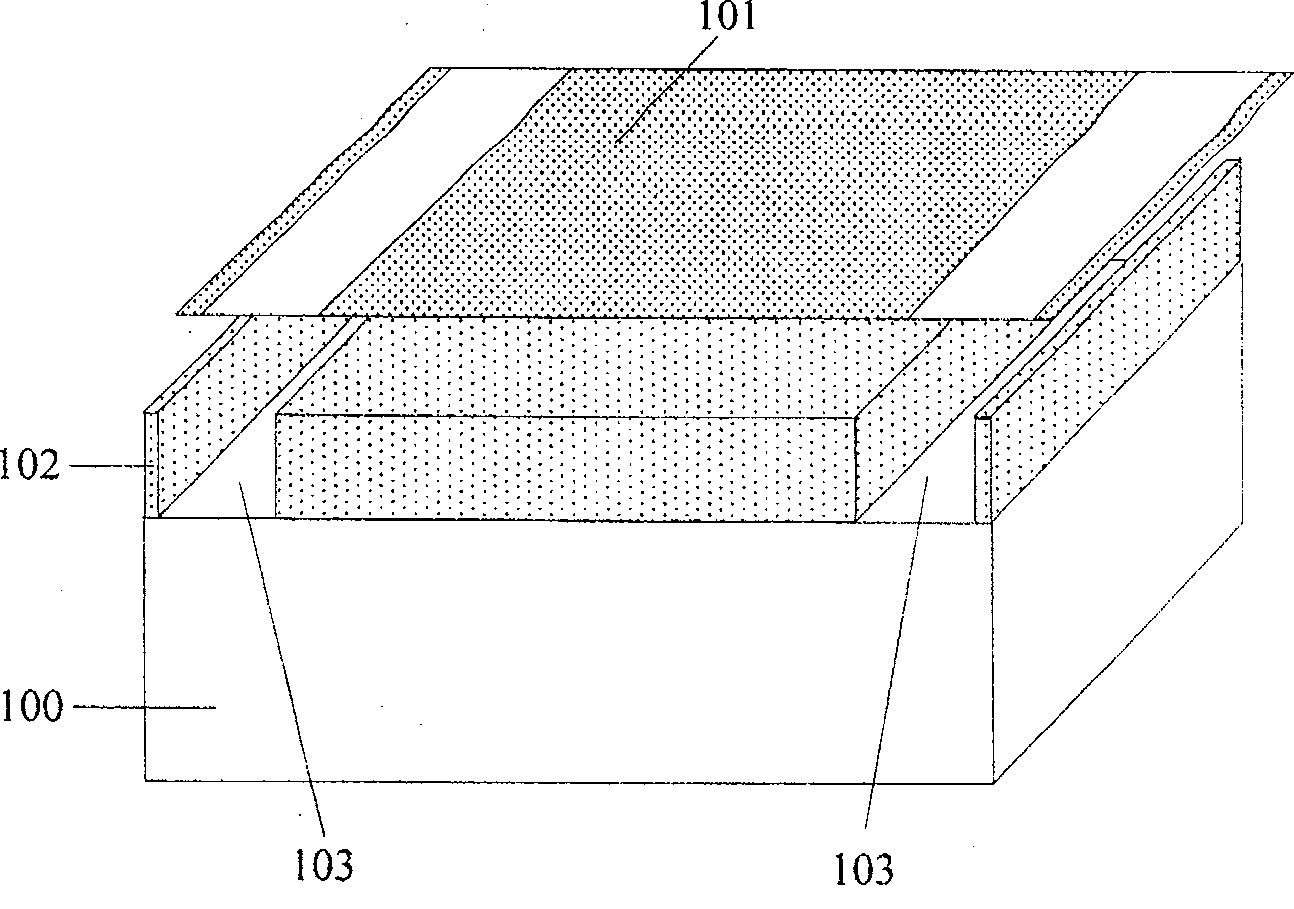
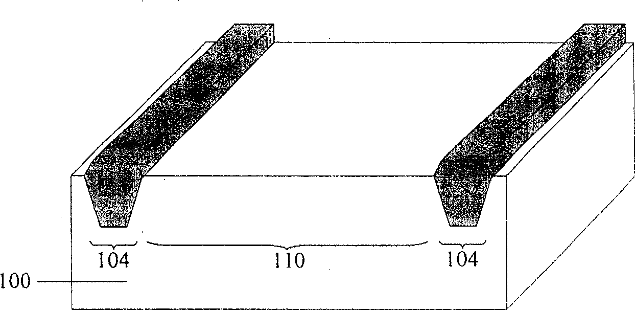
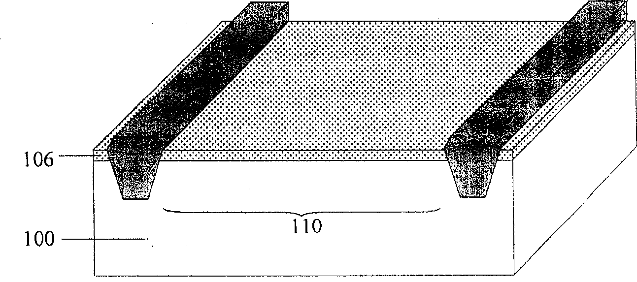
[0030] In the existing process of manufacturing the gate oxide layer of the MOS transistor, since the gate oxide layer of the high-voltage MOS transistor is relatively thick and is affected by the chamfering of the shallow trench isolation region, and is affected by the chamfering of the shallow trench isolation region, the formation of the gate oxide layer During the process, it is easy to cause the edge part of the gate oxide layer to be thinner than the middle part, resulting in a decrease in the threshold voltage at the edge of the gate oxide layer, resulting in a double peak phenomenon, resulting in high power consumption of the device and poor stability of the device operation. In the present invention, in the graphic layout software, an auxiliary active area graphic to be exposed is formed at the junction of the active area graphic to be exposed and the isolated area graphic to be exposed, which is connected with the active area graphic to be exposed and protrudes toward ...


PUM


Abstract

A method for manufacturing a high-voltage MOS transistor, comprising the following steps: forming an auxiliary active region pattern to be exposed at the junction of an active region pattern to be exposed and an isolation region pattern to be exposed, and the auxiliary active region pattern to be exposed and the pattern to be exposed The pattern of the active region is connected to the pattern of the isolation region to be exposed; the pattern of the active region to be exposed, the pattern of the isolation region to be exposed and the pattern of the auxiliary active region to be exposed are transferred to the silicon substrate to form the active region, the isolation region and the auxiliary region. Active region; forming a gate oxide layer on the silicon substrate of the active region and the auxiliary active region; forming a polysilicon layer on the gate oxide layer; forming an opening pattern to be exposed in the gate pattern to be exposed; The pattern and the pattern of the opening to be exposed are transferred to the polysilicon layer to form a gate including an opening, the opening completely exposes the auxiliary active region, and the overlapping part of the gate and the active region is a channel. After the above steps, the bimodal phenomenon will not appear, thereby reducing the power consumption of the device and increasing the stability of the device operation.

Description

technical field [0001] The invention relates to a semiconductor manufacturing process, in particular to a method for manufacturing a high-voltage MOS transistor, in particular to a method for preventing double-peak effects in the process of manufacturing a high-voltage MOS transistor. Background technique [0002] In semiconductor technology, even though the device size continues to shrink, it is still desirable to improve the performance of transistors, and it is also desirable to manufacture integrated circuit semiconductor devices that combine low, high, and medium voltage applications. For example, integrated circuits (hereinafter referred to as driver ICs) used to drive image sensors, LCDs, and printed magnetic heads, etc., are composed of ICs with strong withstand voltage between the drain and source that operate at a power supply voltage above +V. The drive output unit of the high-voltage MOS transistor and the logic unit of the control drive output unit of the low-vo...

Claims


Application Information

Patent Timeline
Patent Type & Authority Patents(China)
IPC IPC(8): H01L21/336H01L21/822
Inventor 蔡巧明辛春艳卢普生
Owner SEMICON MFG INT (SHANGHAI) CORP
Why Eureka
Try Eureka