Flexible optoelectronic thin membrane and manufacturing method thereof

A photoelectric thin film and photoelectric medium technology, applied in optics, nonlinear optics, instruments, etc., can solve problems such as lack of alignment ability, achieve the effect of improving image brightness and reducing manufacturing costs

Active Publication Date: 2009-09-23
IRIS OPTRONICS INC
View PDF3 Cites 0 Cited by
  • Summary
  • Abstract
  • Description
  • Claims
  • Application Information

AI Technical Summary

Problems solved by technology

[0006] Furthermore, neither the PDLC process, PSLC process, microcapsule method nor microcup method has the ability to align, so only a few types of liquid crystals can be used.
In addition, regardless of the PDLC process, PSLC process, microcapsule method and microcup method, it is impossible to directly contact the conductive electrode with the photoelectric medium.

Method used


Image

  • Flexible optoelectronic thin membrane and manufacturing method thereof
  • Flexible optoelectronic thin membrane and manufacturing method thereof
  • Flexible optoelectronic thin membrane and manufacturing method thereof

Examples


Embodiment Construction

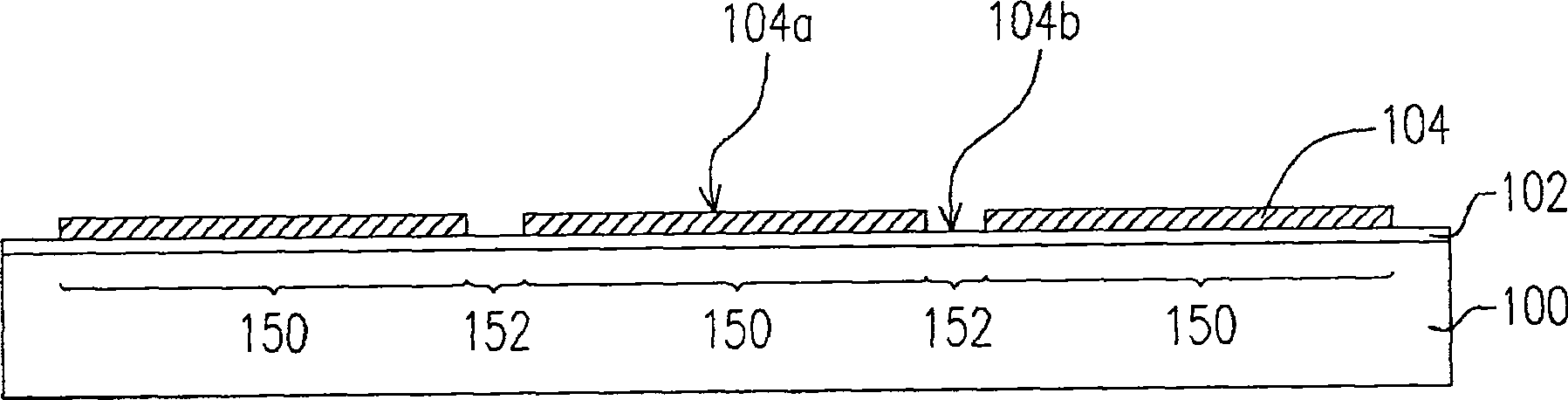
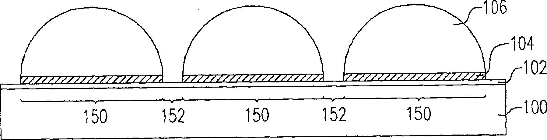
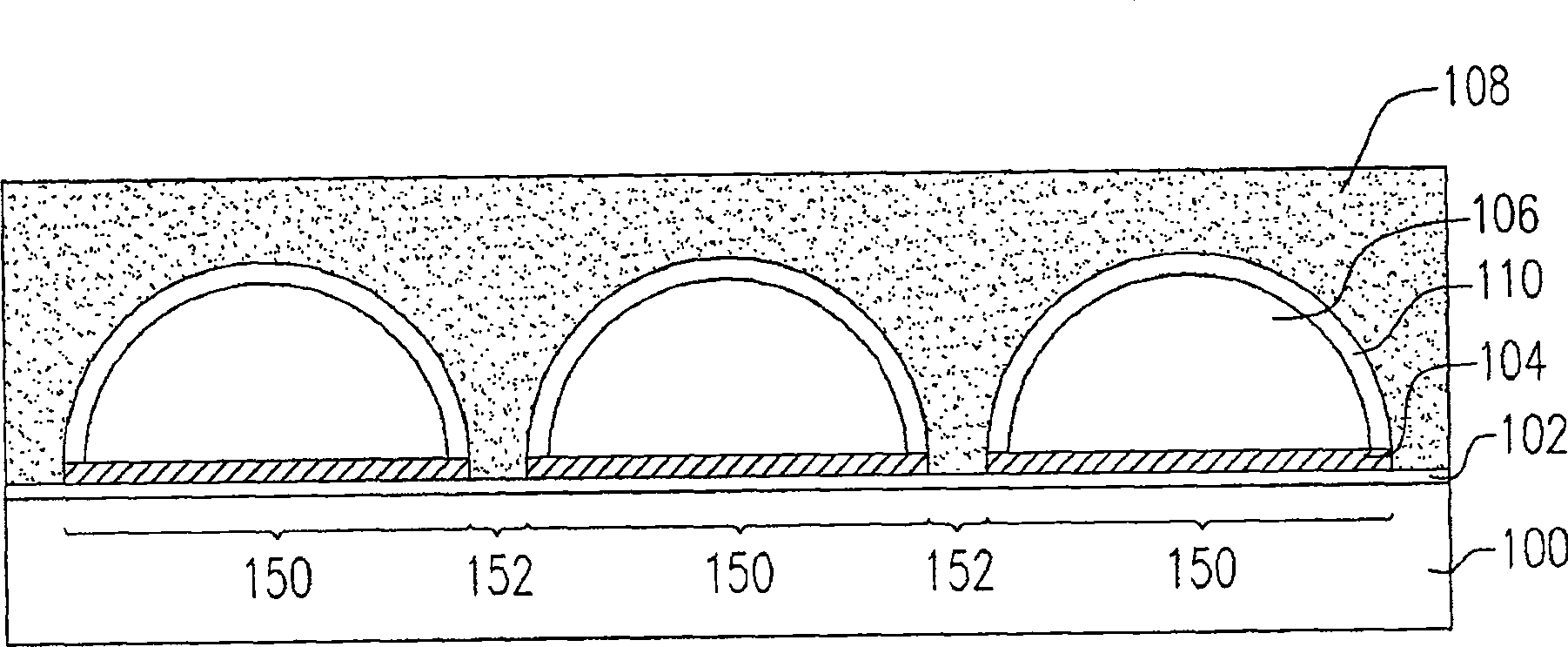
[0057] Figures 1A to 1G Illustrated is a schematic cross-sectional view of a method for manufacturing a flexible photoelectric thin film according to an embodiment of the present invention. Such as Figure 1A As shown, a substrate 100 is provided first. Afterwards, a conductive layer 102 is formed on the substrate 100 . The conductive layer 102 is, for example, a full conductive layer or a patterned conductive layer. The substrate 100 is, for example, a flexible or bendable or rigid substrate. The material of the substrate 100 includes plastic, metal, glass and other synthetic materials. The material of the conductive layer 102 includes a transparent conductive material, such as indium tin oxide (ITO), antimony tin oxide, or other synthetic materials. In addition, the material of the conductive layer 102 can also be a metal material, such as aluminum, copper, silver, molybdenum, chromium and the like. In addition, the material of the conductive layer 102 can also be a co...


PUM

PropertyMeasurementUnit
heightaaaaaaaaaa

Abstract

A method for forming a flexible photoelectric thin film, the method includes: providing a first substrate, wherein a conductive layer is provided on the first substrate. Afterwards, a first positioning structure is formed on the conductive layer, wherein the first positioning structure includes a plurality of first target areas and a plurality of first peripheral areas located around the first target areas, and the surface tension of the first target areas is Different from the surface tension of the first peripheral zone. Next, an electro-optic medium placement process is performed to form electro-optic medium droplets on each of the first target areas. Next, a curing process is performed to respectively form a film wall covering each droplet of the first electro-optic medium. Finally, pressing the first substrate and the second substrate.

Description

technical field [0001] The invention relates to an electronic component and its manufacturing method, and in particular to a flexible photoelectric thin film and its manufacturing method. Background technique [0002] There are currently several approaches claiming to fabricate flexible displays in a roll-to-roll process. Among the technologies currently developed for manufacturing flexible displays, the industry mostly uses polymer dispersed liquid crystal display (PDLC) technology, polymer stabilized liquid crystal display (PSLC) technology, Microcapsule (microcapsule) method and microcup (microcup) method. [0003] Regarding the PDLC process and the PSLC process, because it is not easy to control the distribution of the polymer phase and the liquid crystal phase, the displays manufactured by PDLC and PSLC have disadvantages such as low contrast and high driving voltage. [0004] As far as the microcapsule method is concerned, since it is difficult to produce a uniform s...

Claims


Application Information

Patent Timeline
Patent Type & Authority Patents(China)
IPC IPC(8): G02F1/01G02F1/13G02F1/167G02F1/15
Inventor 侯维新丁兆民王兴龙廖奇璋林雁容
Owner IRIS OPTRONICS INC
Why Eureka
Try Eureka