Image sensor device and fabrication method thereof

A technology for image sensing devices and manufacturing methods, which is applied in radiation control devices, semiconductor/solid-state device manufacturing, printed circuit assembly of electrical components, etc., can solve problems such as impact and poor device performance, and achieve the effect of reducing manufacturing costs

Active Publication Date: 2009-09-23
VISERA TECH CO LTD +1
View PDF6 Cites 2 Cited by
  • Summary
  • Abstract
  • Description
  • Claims
  • Application Information

AI Technical Summary

Problems solved by technology

Therefore, if the packaged modules or electronic components cannot be designed with EMI protection, the performance of the device will be adversely affected

Method used


Image

  • Image sensor device and fabrication method thereof
  • Image sensor device and fabrication method thereof
  • Image sensor device and fabrication method thereof

Examples


Embodiment Construction

[0021] The manufacture and use of the embodiments of the present invention are described below. It should be readily appreciated, however, that the present invention provides many applicable inventive concepts that can be implemented in a wide variety of specific contexts. The specific embodiments are only used to illustrate the manufacture and use of the present invention in a specific way, and are not intended to limit the scope of the present invention.

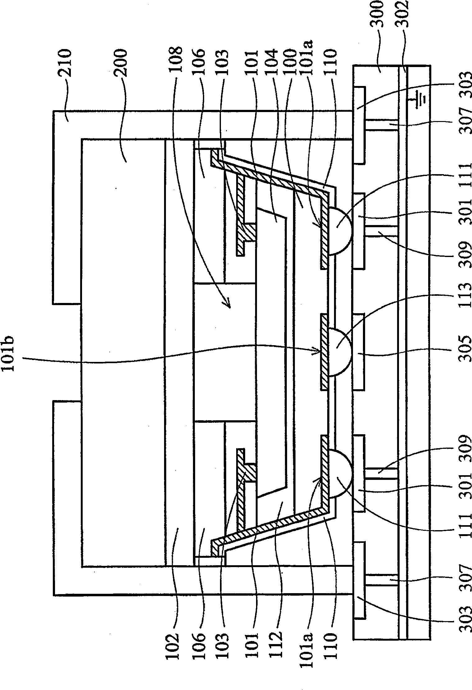
[0022] figure 1 Shows the electronic components used in image sensing devices known to the inventors of the present invention, which are not prior art for determining the patentability of the present invention, but only to demonstrate the problems discovered by the inventors of the present invention .

[0023] Please refer to figure 1 , the electronic component includes an image sensor chip scale package (chip scale package, CSP) module and a lens group 200 , which are sequentially assembled on a printed circuit board (...


PUM


Abstract

The invention provides an electronic component of an image sensing device, comprising: a packaging module, a lens group, a non-transparent conductive layer, a printed circuit board, and solder balls; The first conductive layer, the first protective layer and the first pad; the lens group is assembled on the packaging module; the non-transparent conductive layer is arranged on the side wall of the lens group and is electrically connected to the first conductive layer; the printed circuit board, Assembled in the encapsulation module and having a ground layer disposed inside; and solder balls disposed on the first pad and electrically connected to the ground layer. The present invention can solve the EMI problem without using a metal case for EMI protection, thereby reducing the manufacturing cost.

Description

technical field [0001] The present invention relates to an image sensing device technology, in particular to a packaging module and an electronic component with electromagnetic interference (electromagnetic interference, EMI) protection for an image sensing device. Background technique [0002] Charge-coupled device (CCD) image sensing devices and complementary metal oxide semiconductor (CMOS) image sensing devices are widely used in digital image products. Image capture techniques are also well known to consumers due to the increased usage of image sensing devices such as digital cameras, digital image recorders, camera phones and monitors, among others. [0003] An image sensing device typically includes a diode array for pixels, a control circuit, an analog-to-digital converter, and an amplifier. Regardless of whether these devices are on the same chip, such as a sensor device, or in a camera module or on a printed circuit board (PCB), preventing electromagnetic interfer...

Claims


Application Information

Patent Timeline
Patent Type & Authority Patents(China)
IPC IPC(8): H01L27/146H01L23/552H01L21/50H05K1/18H05K3/32H05K9/00
CPCH01L2224/11H01L2224/16225
Inventor 陈腾盛戎柏忠林孜翰熊信昌
Owner VISERA TECH CO LTD
Why Eureka
Try Eureka