
Method for manufacturing three-dimensional nerve microelectrode

A manufacturing method and micro-electrode technology, which are applied in the directions of micro-structure technology, micro-structure device, manufacturing micro-structure device, etc., can solve the problems of large influence of insulating layer process, unfavorable long-term implantation, easy generation of pinholes, etc., and achieve the production cost. reduction, good electrical uniformity, pinhole elimination effect

Active Publication Date: 2009-10-21
上海华实投资有限公司
View PDF4 Cites 0 Cited by
  • Summary
  • Abstract
  • Description
  • Claims
  • Application Information

AI Technical Summary

Problems solved by technology

[0003] Found through literature search to prior art, Peter Norlin et al published on Journal ofmicromechanics and Microengineering (micromechanics and microengineering periodical) (2002, 12 phases, 414-419 pages) ("A 32-site neural recording probe fabricated by DRIE of SOI substrates") (fabrication of 32 recording point electrodes on SOI substrates), this article proposes to use silicon deep etching process to fabricate silicon microelectrodes, the specific method is to use deep reactive ion etching (DRIE) technology to determine the electrode structure, SiO 2 and Si 3 N 4 As an electrical insulating layer, its disadvantage is that the microelectrode is a planar structure, and the insulating layer is greatly affected by the process, which is prone to pinholes, which is not conducive to long-term implantation in the body.

Method used


Image

  • Method for manufacturing three-dimensional nerve microelectrode
  • Method for manufacturing three-dimensional nerve microelectrode

Examples


Embodiment 1

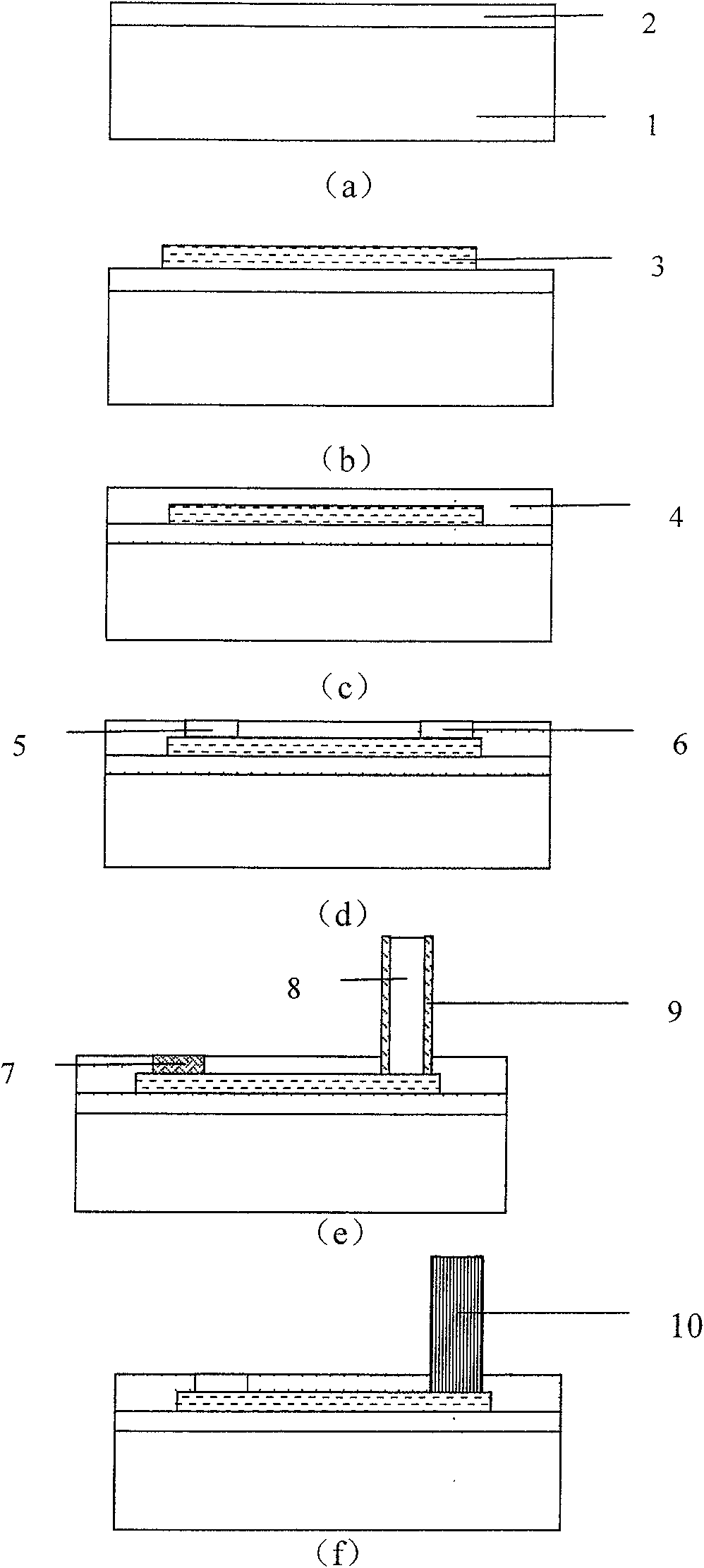
[0025] In this embodiment, the cylindrical hole 8 made of SU-8 glue has a height of 100 micrometers and is used for sticking on the surface of the dura mater of the optic nerve or cerebral cortex to stimulate the optic nerve or cerebral cortex to restore nerve function.

[0026] Such as figure 1 As shown, this embodiment includes the following steps:

[0027] Step 1, clean the silicon wafer 1, use the silicon wafer 1 as the substrate, and use PECVD (plasma chemical vapor deposition) method to grow the bottom SiO on the polished surface of the silicon wafer 1 2 2. Bottom SiO2 2 2 for electrically isolating the metal alloy layer from the silicon substrate, such as figure 1 (a) shown.

[0028] The silicon wafer 1 is N-type single crystal silicon.

[0029] Step 2, on the bottom SiO 2 Metal titanium and gold are sequentially sputtered on 2 to form a metal alloy layer, and metal interconnection lines 3, pads 5 and contact dots 6 are etched out. Dot 6 is used for electroplatin...

Embodiment 2

[0036] In this embodiment, the cylindrical hole 8 made of SU-8 glue has a height of 500 micrometers and is used to penetrate the dura mater and stick on the surface of the pia mater to stimulate the optic nerve or cerebral cortex to restore nerve function.

[0037] Such as figure 1 As shown, this embodiment includes the following steps:

[0038] Step 1, clean the silicon wafer 1, use the silicon wafer 1 as the substrate, and use PECVD (plasma chemical vapor deposition) method to grow the bottom SiO on the polished surface of the silicon wafer 1 2 2. Bottom SiO2 2 2 for electrically isolating the metal alloy layer from the silicon substrate, such as figure 1 (a) shown.

[0039] The silicon wafer 1 is P-type single crystal silicon.

[0040] Step 2, on the bottom SiO 2Metal titanium and gold are sequentially sputtered on 2 to form a metal alloy layer, and metal interconnection lines 3, pads 5 and contact dots 6 are etched out. Dot 6 is used for electroplating to grow cylind...

Embodiment 3

[0047] The height of the cylindrical hole 8 that adopts SU-8 glue to form among the present embodiment is 1 millimeter, is used for penetrating dura mater and pia mater, punctures in optic nerve or cerebral cortex, is used for stimulating optic nerve or cerebral cortex, carries out neural Functional fixes.

[0048] Such as figure 1 As shown, this embodiment includes the following steps:

[0049] Step 1, clean the silicon wafer 1, use the silicon wafer 1 as the substrate, and use PECVD (plasma chemical vapor deposition) method to grow the bottom SiO on the polished surface of the silicon wafer 1 2 2. Bottom SiO2 2 2 for electrically isolating the metal alloy layer from the silicon substrate, such as figure 1 (a) shown.

[0050] The silicon wafer 1 is N-type single crystal silicon.

[0051] Step 2, on the bottom SiO 2 Metal titanium and gold are sequentially sputtered on 2 to form a metal alloy layer, and metal interconnection lines 3, pads 5 and contact dots 6 are etched ...


PUM


Abstract

A method for manufacturing a three-dimensional neural microelectrode in the field of micro-electromechanical technology, specifically as follows: a silicon wafer is used as a substrate, and a bottom SiO2 is grown on the front side of the silicon wafer; a metal alloy layer is formed on the bottom SiO2, and metal interconnections are etched out Lines, pads and contact dots; the top layer of SiO2 is grown on the front side of the bottom SiO2, and the top layer of SiO2 is etched with buffered HF acid solution to expose the pads and contact dots, and the pads are filled with photoresist; Spin-coat SU-8 glue on the front side of the silicon planar structure in contact with the dots, and form cylindrical holes through photolithography and etching processes, fill the pads with photoresist; grow metal in the cylindrical holes by electroplating to form metal cylinders , using a development method to remove the photoresist in the pads to expose the pads; and cleaning to obtain a three-dimensional multi-channel micro-electrode array. The invention reduces the production cost, improves the controllability of the micro-electrodes and the consistency of each channel.

Description

technical field [0001] The invention relates to a processing method in the field of micro-electromechanical technology, in particular to a method for manufacturing a three-dimensional nerve microelectrode based on a micro-electromechanical processing technology. Background technique [0002] For many patients with severe neurological damage, traditional drug therapy and other methods cannot cure nerve damage. At the same time, nerve repair methods based on artificial electronic devices have been widely studied and applied. As the interface components between artificial electronic devices and biological tissues, neural microelectrodes are playing an increasingly important role in the field of neural repair such as motor function and sensory function. In the study of artificial hearing restoration, microelectrodes implanted in the cochlea are used to directly stimulate the remaining auditory nerve fibers, and send neural electrical signals to the auditory center of the brain t...

Claims


Application Information

Patent Timeline
Patent Type & Authority Patents(China)
IPC IPC(8): B81C1/00
Inventor 隋晓红李莹辉任秋实
Owner 上海华实投资有限公司
Learn More