Planar display and chip joint pad

A flat-panel display and chip bonding technology, which is applied in the fields of instruments, nonlinear optics, optics, etc., can solve the problems of high material cost requirements and high transmission impedance of flexible circuit boards and control circuit boards

Active Publication Date: 2009-12-09
AU OPTRONICS CORP
View PDF5 Cites 0 Cited by
  • Summary
  • Abstract
  • Description
  • Claims
  • Application Information

AI Technical Summary

Problems solved by technology

[0009] The purpose of the present invention is to provide a flat-panel display, which can solve the problem that the traditional flat-panel display requires a large material cost for the flexible circuit board and the control circuit board
[0010] Another object of the present invention is to provide a chip bonding pad, which can solve the problem of high transmission impedance in traditional chip bonding pads

Method used


Image

  • Planar display and chip joint pad
  • Planar display and chip joint pad
  • Planar display and chip joint pad

Examples


Embodiment Construction

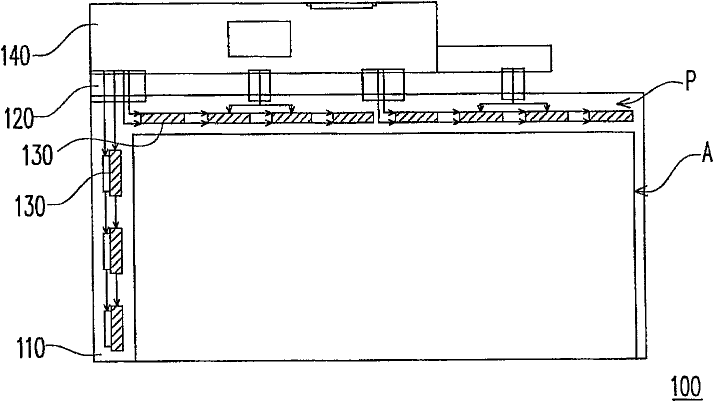
[0053] Figure 2A An example of the liquid crystal display of the present invention is shown. Please refer to Figure 2A , the flat panel display 200 includes: a display panel 210, a flexible circuit board 220, a plurality of gate driver chips 230, a plurality of first source driver chips 240, a plurality of second source driver chips 250, and a control circuit board 260 . The control circuit board 260 is electrically connected to the flexible circuit board 220 . The display panel 210 includes: a display area A and a peripheral circuit area P. The gate driver chip 230 , the first source driver chip 240 and the second source driver chip 250 are all disposed in the peripheral circuit region P. As shown in FIG.

[0054] The display panel 210 has a plurality of first wires 212A and second wires 212B located in the peripheral circuit area P. The flexible circuit board 220 is electrically connected to the first wire 212A and the second wire 212B, wherein the first wire 212A and...


PUM


Abstract

A plane display and its chip bonding pads. The plane display includes a display panel, a flexible circuit board, a first source driver chip, a second source driver chip and a control circuit board. There are a plurality of first wires and second wires in the peripheral circuit area of ​​the display panel, the first wires and the second wires respectively extend from the bottom of the flexible circuit board to the two opposite sides of the display panel, and are connected with the flexible circuit board electrical connection. The first source driver chip is electrically connected to the flexible circuit board through a part of the first wire. The second source driver chip is electrically connected to the flexible circuit board through the second wire. The chip bonding pad is located under the first source driver chip or the second source driver chip, the first dielectric layer has a plurality of first contact openings, and the second dielectric layer has a plurality of alternately arranged second contact openings and the third contact opening, and the second contact opening corresponds to the first contact opening.

Description

technical field [0001] The invention relates to a flat display and a chip bonding pad, and in particular to a flat display with signal transmission impedances matched to each other and a chip bonding pad with low signal transmission impedance. Background technique [0002] With the development of the information industry, the requirements for the volume occupied by various displays in the market are getting higher and higher, and therefore various displays are constantly developing towards thinning. For example, flat panel displays such as liquid crystal displays and organic light emitting displays have replaced traditional picture tube displays and become mainstream products of displays. [0003] Figure 1A It is a schematic diagram of a traditional flat panel display. Please refer to Figure 1A , the flat panel display 100 includes a display panel 110 , a plurality of flexible circuit boards 120 , a plurality of driving chips 130 and a control circuit board 140 . The dis...

Claims


Application Information

Patent Timeline
Patent Type & Authority Patents(China)
IPC IPC(8): G02F1/13
Inventor 刘俊欣刘柏源
Owner AU OPTRONICS CORP
Why Eureka
Try Eureka