Large power beam coupled semiconductor laser

A semiconductor and laser technology, applied in the field of high-power semiconductor lasers, can solve the problems of large divergence angle, reduced efficiency of half-wave plate rotating polarization direction, complicated adjustment, etc., to achieve high output power and brightness, reduce the difficulty of device adjustment, and improve coupling. The effect of efficiency

Inactive Publication Date: 2009-12-30
CHANGCHUN INST OF OPTICS FINE MECHANICS & PHYSICS CHINESE ACAD OF SCI
View PDF2 Cites 4 Cited by
  • Summary
  • Abstract
  • Description
  • Claims
  • Application Information

AI Technical Summary

Problems solved by technology

This structure can achieve beam combining, but the disadvantages are: (1) The two lasers are placed vertically at 90°, and the adjustment is complicated; (2) The cube polarization coupling prism is used, and the middle glued surface melts the glue during long-term high-power use, which improves the efficiency. (3) Due to the large divergence angle of the semiconductor laser itself without collimation, the efficiency of directly placing the half-wave plate to rotate the polarization direction is reduced
(4) The distance between the cube polarization coupling prism and the half-wave plate is large, the coupling efficiency is low, and it is difficult to adjust
(5) Cube polarization coupling prism is used as coupling, which is expensive

Method used


Image

  • Large power beam coupled semiconductor laser
  • Large power beam coupled semiconductor laser
  • Large power beam coupled semiconductor laser

Examples


Embodiment Construction

[0013] The present invention will be described in further detail below in conjunction with the embodiment given with accompanying drawing.

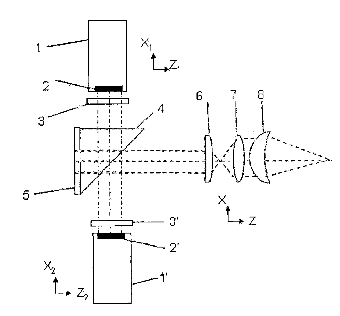
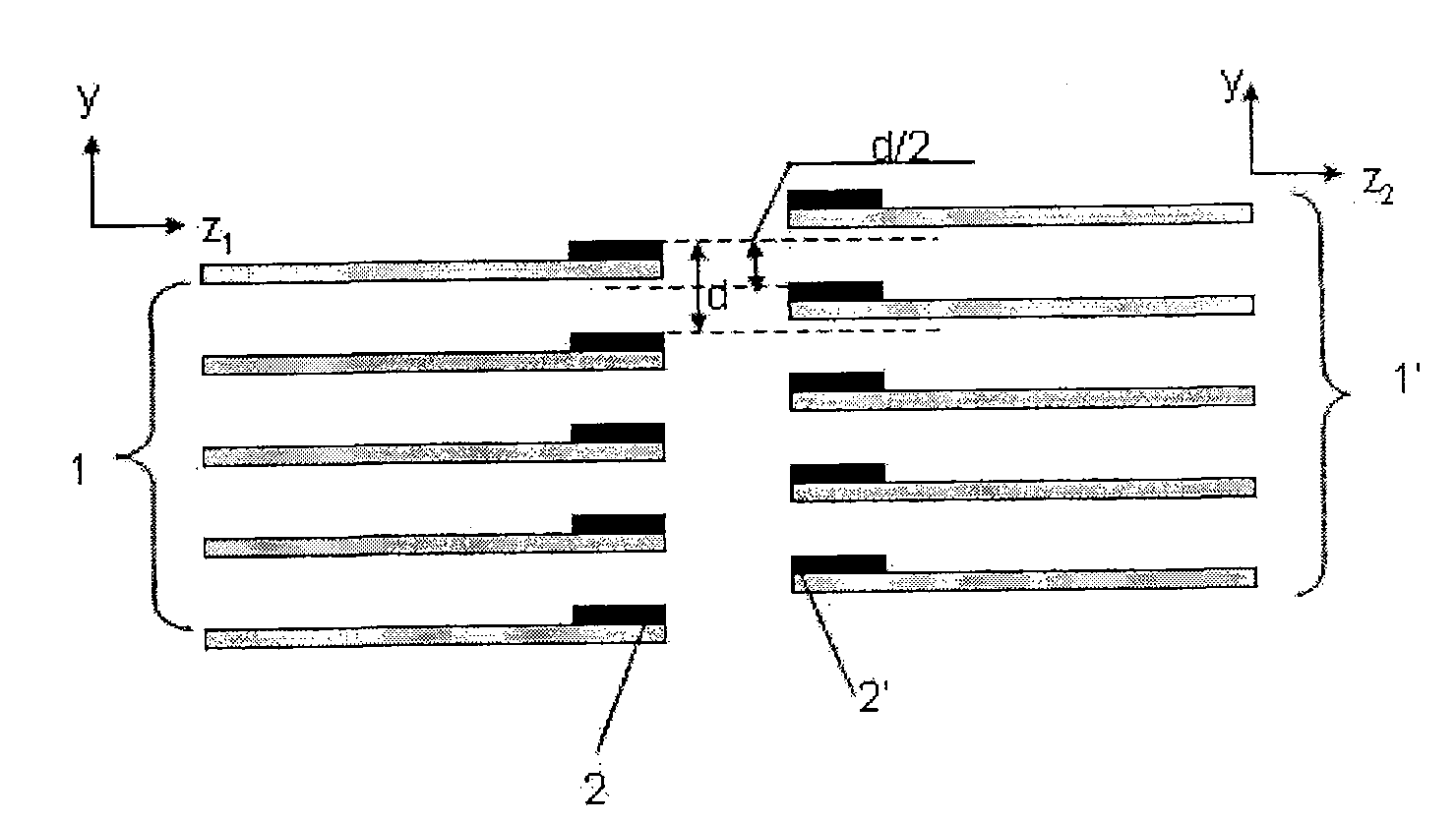
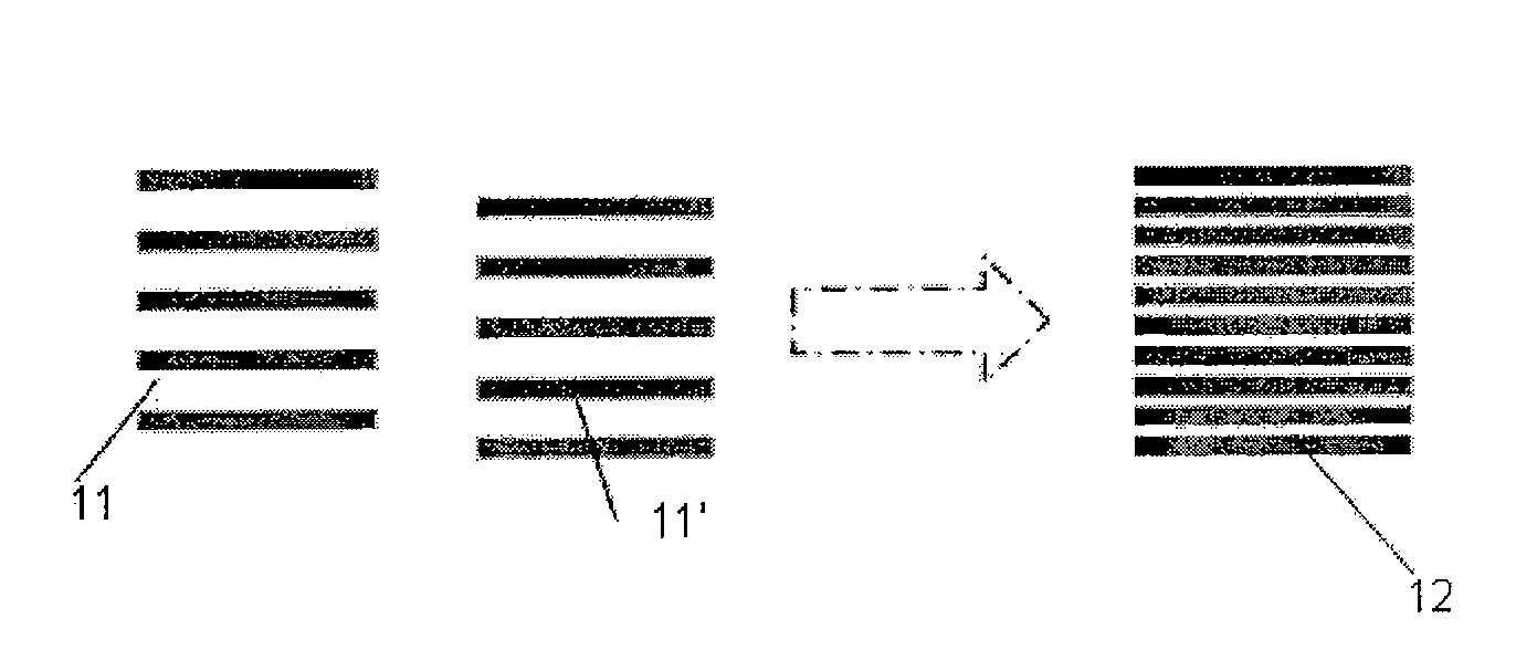
[0014] refer to figure 1 , including two semiconductor lasers 1, 1' with the same wavelength and the same polarization state, and a beam expander focusing device, it is characterized in that: the two semiconductor lasers 1, 1' are relatively placed on the same optical axis, and the two semiconductor lasers 1 On the optical path between , 1', a right-angled polarization coupling prism 4 coated with a polarizing film is set on its slope, and a quarter-wave plate 5 is pasted on one side of the right-angled polarization coupling prism 4 at a right angle. The outer end surface of one of the wave plates 5 is coated with a high-reflection film, and the outgoing beam of a laser 1' is reflected by the slope of the right-angled polarization coupling prism 4 to rotate the transmission direction by 90 degrees and then transmitted to the beam expande...


PUM


Abstract

The invention relates to a high-power semiconductor laser device, especially a high-power light beam coupling semiconductor laser device, including two semiconductor laser devices with same wavelength and polarization state, a beam-expanding focusing device. The two semiconductor laser devices are deposited relatively on an optical axis, a right-angle polarization coupling prism with polarization membranous on its inclined surface is arranged on an optical path between the two semiconductor laser devices, a quarter wave plate is pasted on one right-angle surface of the right-angle polarization coupling prism, an emergent light beam of the laser is transmitted to the beam-expanding focusing device after reflecting by the right-angle polarization coupling prism, and the emergent light beam of the other laser is coupled to a beam to transmit after 90 DEG rotation of polarization direction by reflecting of the quarter wave plate. The paste placement of the quarter wave plate and the right-angle polarization coupling prism, and reduces device regulation difficulty and improves coupling efficiency, also improves the output power and lightness by two times without changing light beam quality.

Description

technical field [0001] The invention relates to a high-power semiconductor laser, in particular to a high-power laser realized by coupling the light beams of two semiconductor laser light sources. Background technique [0002] Compared with other types of lasers, semiconductor lasers (LD) have the advantages of small size, light weight, high efficiency, long life, and direct current modulation, so they are widely used in many fields such as industry, military, nuclear energy, and communications. The requirements for output power and brightness of semiconductor lasers are also getting higher and higher. By integrating the semiconductor laser light-emitting unit into a one-dimensional line array (LD Bar) and a two-dimensional array (LD Stack) stacking multiple LD Bars, the output power of the semiconductor laser can be effectively improved, but due to the limitation of heat dissipation, the two Dimensional area arrays cannot stack LD Bars without limitation. Internationally, ...

Claims


Application Information

Patent Timeline
Patent Type & Authority Patents(China)
IPC IPC(8): H01S5/40
Inventor 顾媛媛彭航宇王立军单肖楠刘云王祥鹏
Owner CHANGCHUN INST OF OPTICS FINE MECHANICS & PHYSICS CHINESE ACAD OF SCI
Why Eureka
Try Eureka