Electroplating method

A technology of electroplating equipment and electrodes, which is applied in the manufacture of circuits, electrical components, semiconductors/solid-state devices, etc. It can solve the problems of electroplating solution aging and inability to solve many particle defects on the surface of the wafer, so as to increase humidity, reduce electrolyte volume, The effect of increasing the range

Inactive Publication Date: 2010-02-17
SEMICON MFG INT (SHANGHAI) CORP +1
View PDF5 Cites 0 Cited by
  • Summary
  • Abstract
  • Description
  • Claims
  • Application Information

AI Technical Summary

Problems solved by technology

[0011] The Chinese patent application with the publication number CN1536101A published on October 13, 2004 proposed a new electroplating equipment, which provided an accommodating space in the electroplating tank to reduce the large amount of electroplating solution in contact with air, resulting in electroplating solution Phenomena of aging and deterioration
However, it cannot solve the above-mentioned problem of multiple particle defects on the surface of the wafer after electroplating.

Method used


Image

  • Electroplating method
  • Electroplating method
  • Electroplating method

Examples


Embodiment Construction

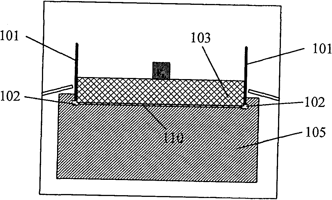
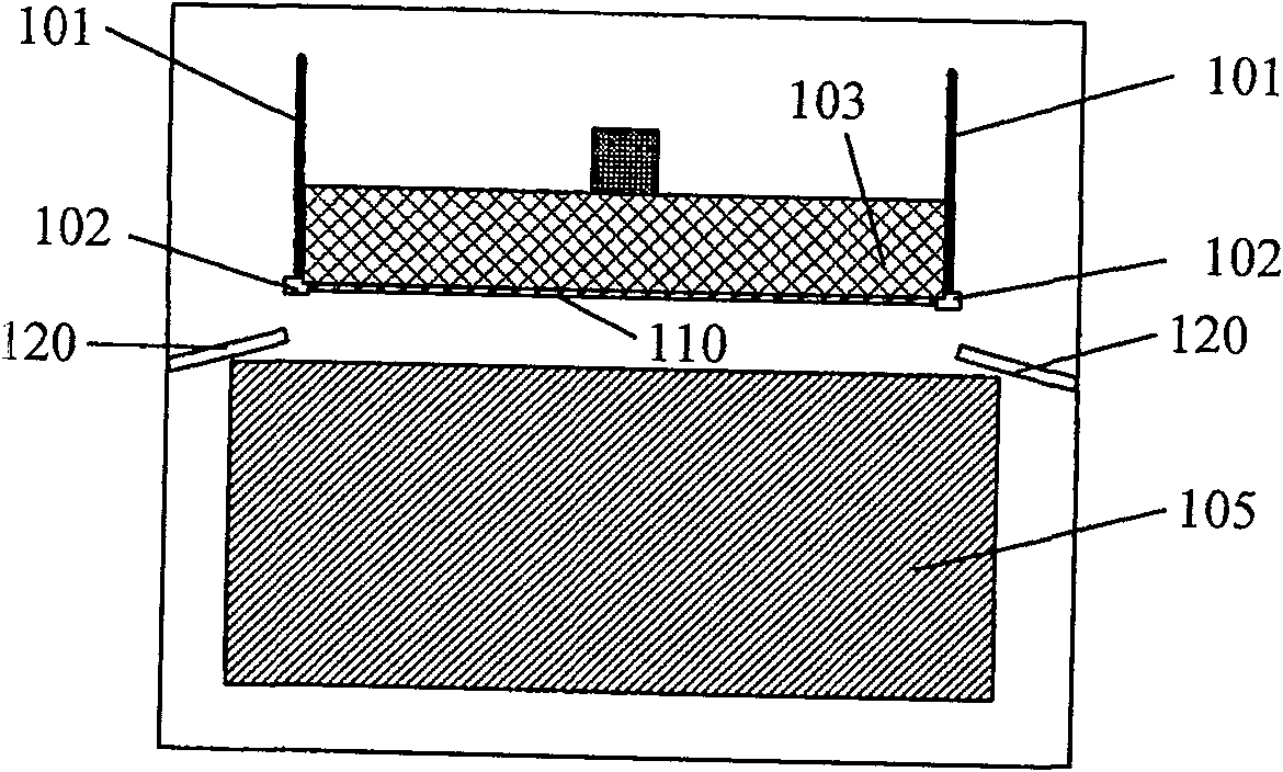
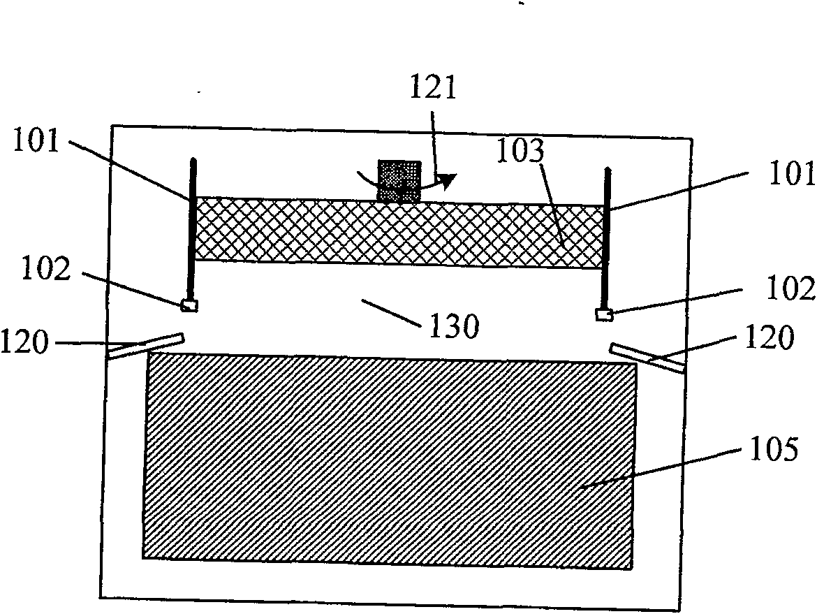
[0049] In order to make the above objects, features and advantages of the present invention more comprehensible, specific implementations of the present invention will be described in detail below in conjunction with the accompanying drawings.

[0050] The processing method of the present invention can be widely used in each field, is described below by specific embodiment, certainly the present invention is not limited to this specific embodiment, the general knowledge well known to those of ordinary skill in the art Substitutions are undoubtedly within the scope of the present invention.

[0051] Secondly, the present invention is described in detail using schematic diagrams. When describing the embodiments of the present invention in detail, for the convenience of explanation, the schematic diagrams showing the structure of the equipment will not be partially enlarged according to the general scale, which should not be used as a limitation of the present invention. In additi...


PUM


Abstract

The invention discloses an electroplating method, which comprises the following steps: putting a wafer to be electroplated into electroplating equipment; descending electrodes and a head cover of theelectroplating equipment to make the electrodes and the wafer immersed into electrolyte in an electrolytic bath of the electroplating equipment; applying current between the electrodes; stopping applying the current between the electrodes; lifting the electrodes and the head cover; washing the wafer by using a water pipe in the electroplating equipment; stopping washing, and performing dry treatment on the wafer; taking off the wafer; and descending the head cover. The electroplating method is adopted to effectively reduce particle contaminant capacity of the surface of the wafer subjected tothe electroplating.

Description

technical field [0001] The invention relates to the technical field of semiconductor manufacturing, in particular to an electroplating method. Background technique [0002] As the critical dimensions of devices shrink, the control of contamination on the wafer surface becomes more and more critical. If pollution sources such as particles are introduced during the production process, it may cause open circuit or disconnection of the circuit. Therefore, in semiconductor process manufacturing, how to avoid pollution in process manufacturing must be paid attention to. With the improvement of equipment automation in production, the interaction between personnel and products becomes less, and the focus of preventing particles in production has been more focused on the particles produced by production equipment. [0003] Taking the formation process of the copper layer as an example, after the semiconductor process technology enters 0.18 microns, the method of electro-chemical pla...

Claims


Application Information

Patent Timeline
Patent Type & Authority Patents(China)
IPC IPC(8): H01L21/3205H01L21/321H01L21/768C25D7/12C25D5/48
Inventor 聂佳相
Owner SEMICON MFG INT (SHANGHAI) CORP
Why Eureka
Try Eureka