LCD base plate with anti static guiding barrier

An anti-static and net-guiding technology, which is applied in the direction of static electricity, electrical components, static indicators, etc., can solve the problems of increasing the steps of control components and increasing manufacturing costs, so as to prevent static protection problems, improve static protection performance, and easy to solve The effect of being hit by static electricity

Active Publication Date: 2007-07-25
SHENZHEN SUCCESS ELECTRONICS LTD
View PDF3 Cites 19 Cited by
  • Summary
  • Abstract
  • Description
  • Claims
  • Application Information

AI Technical Summary

Problems solved by technology

[0009] Both of the above two technologies are to add a static control element between the middle area of ​​the liquid crystal panel and the electrostatic discharge area, so that when there is static electricity in the middle area, the static charge in the middle area can be effectively introduced into the electrostatic discharge area, and When there is no static electricity, it can effectively prevent the mutual interference between the two regions. However, this discharge structure needs to increase the steps of forming control elements, thereby increasing the manufacturing cost.

Method used


Image

  • LCD base plate with anti static guiding barrier
  • LCD base plate with anti static guiding barrier

Examples


Embodiment Construction

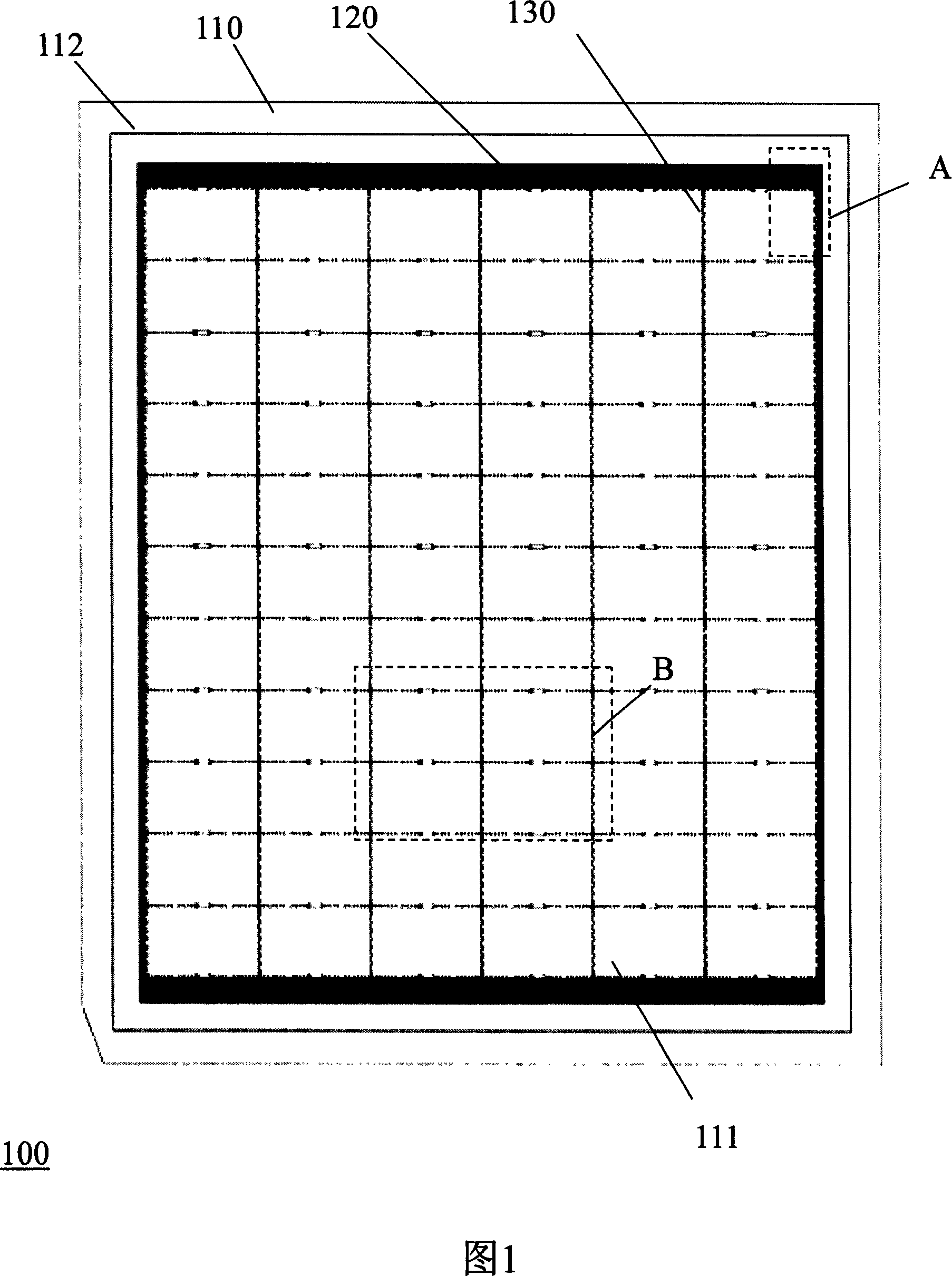
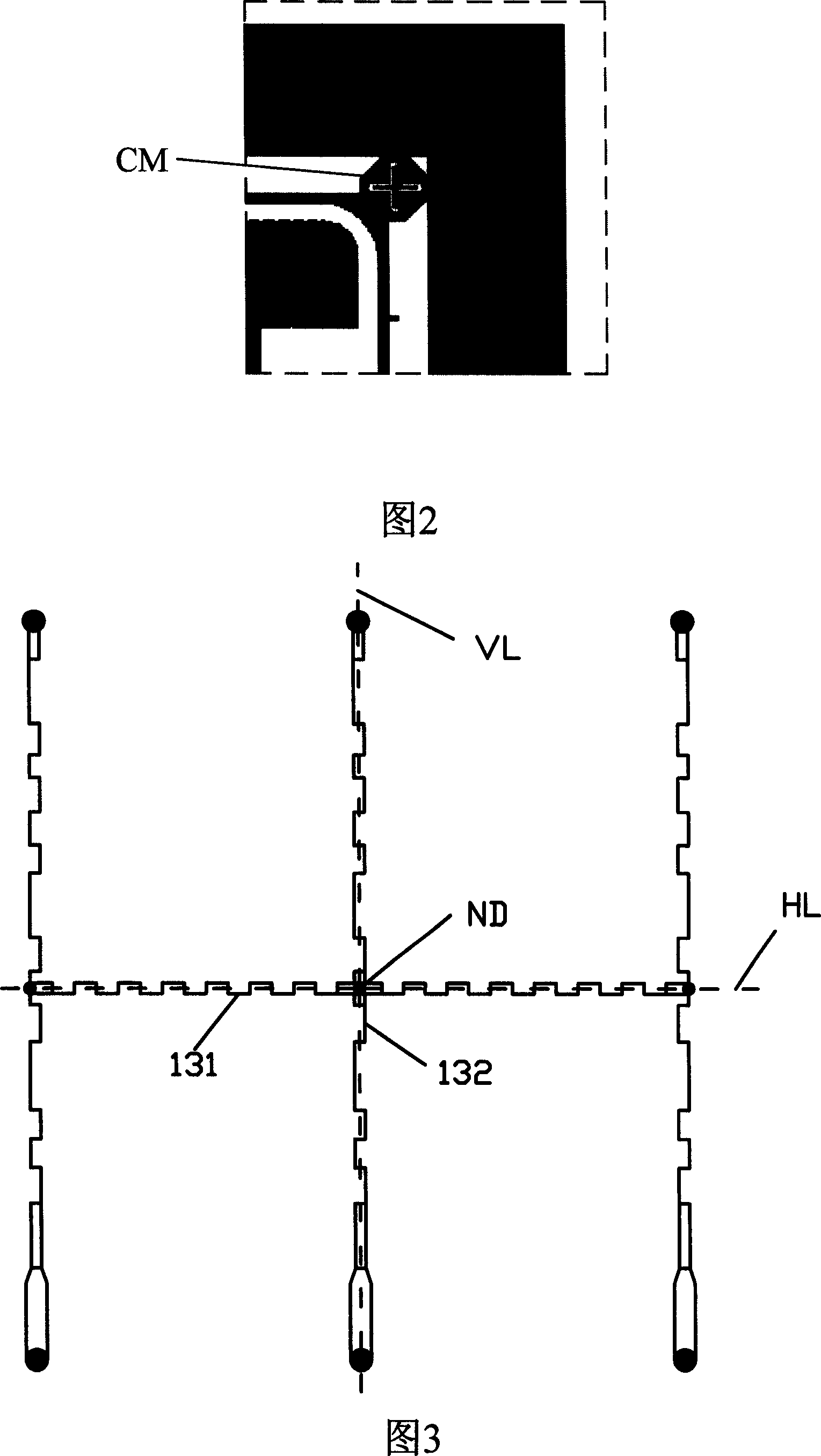
[0020] FIG. 1 is a structural diagram of an LCD substrate with an antistatic guide net according to a specific embodiment of the present invention. Figure 2 and Figure 3 are partial enlarged views. Referring to FIGS. 1 and 3 , an LCD substrate 100 with an antistatic grid includes a substrate 110 , an electrostatic discharge strip 120 , an electrostatic grid 130 , and a plurality of row electrodes and a plurality of column electrodes. Wherein, the substrate 110 has a middle region 111 and a peripheral region 112 , and the peripheral region 112 is adjacent to the middle region 111 . The row electrodes and the column electrodes are disposed in the middle area 111 and are respectively connected to the electrostatic grid 130 .

[0021] In an embodiment of the present invention, the substrate 110 may be made of glass, and the row electrodes and column electrodes may be made of indium tin oxide (ITO), indium zinc oxide (IZO), or other transparent conductive materials. The electrost...


PUM


Abstract

A LCD base plate with static admittance net consists of base plate, multiple line electrodes, multiple column electrode, static releasing belt and static admittance net with multiple level net lines and multiple vertical lines. It is featured as forming multiple node by said level and vertical net lines, superposing said nodes with prefabricated cutting labels, ensuring that said level net lines and vertical net lines are cut to be the first and the second parts being not connected with each other when LCD panel is cut along cutting line defined by cutting label.

Description

technical field [0001] The present invention relates to an LCD panel, and more particularly to an LCD substrate having an electrostatic discharge portion. Background technique [0002] LCD panels in the prior art can be divided into twisted nematic (TN-TwistedNematic), super twisted nematic (STN-Super TN) and double-layer super twisted nematic (DSTN-double-layer STN) according to the working principle And thin film transistor type (TFT-Thin Film Transistor). Among them, the twisted nematic type, super twisted nematic type and double layer super twisted nematic type are called passive display panels, and the thin film transistor type is called active display panels. [0003] For passive LCD panels, the common manufacturing process is to coat a layer of alignment film on the designed metal traces (row electrodes and column electrodes), and then use a rubbing process for alignment to form a specific direction on the LCD metal traces. Layer, to ensure that the liquid crystal m...

Claims


Application Information

Patent Timeline
Patent Type & Authority Applications(China)
IPC IPC(8): G02F1/133G02F1/1333H05F3/00
Inventor 杨顺林宋宇红
Owner SHENZHEN SUCCESS ELECTRONICS LTD
Why Eureka
Try Eureka