

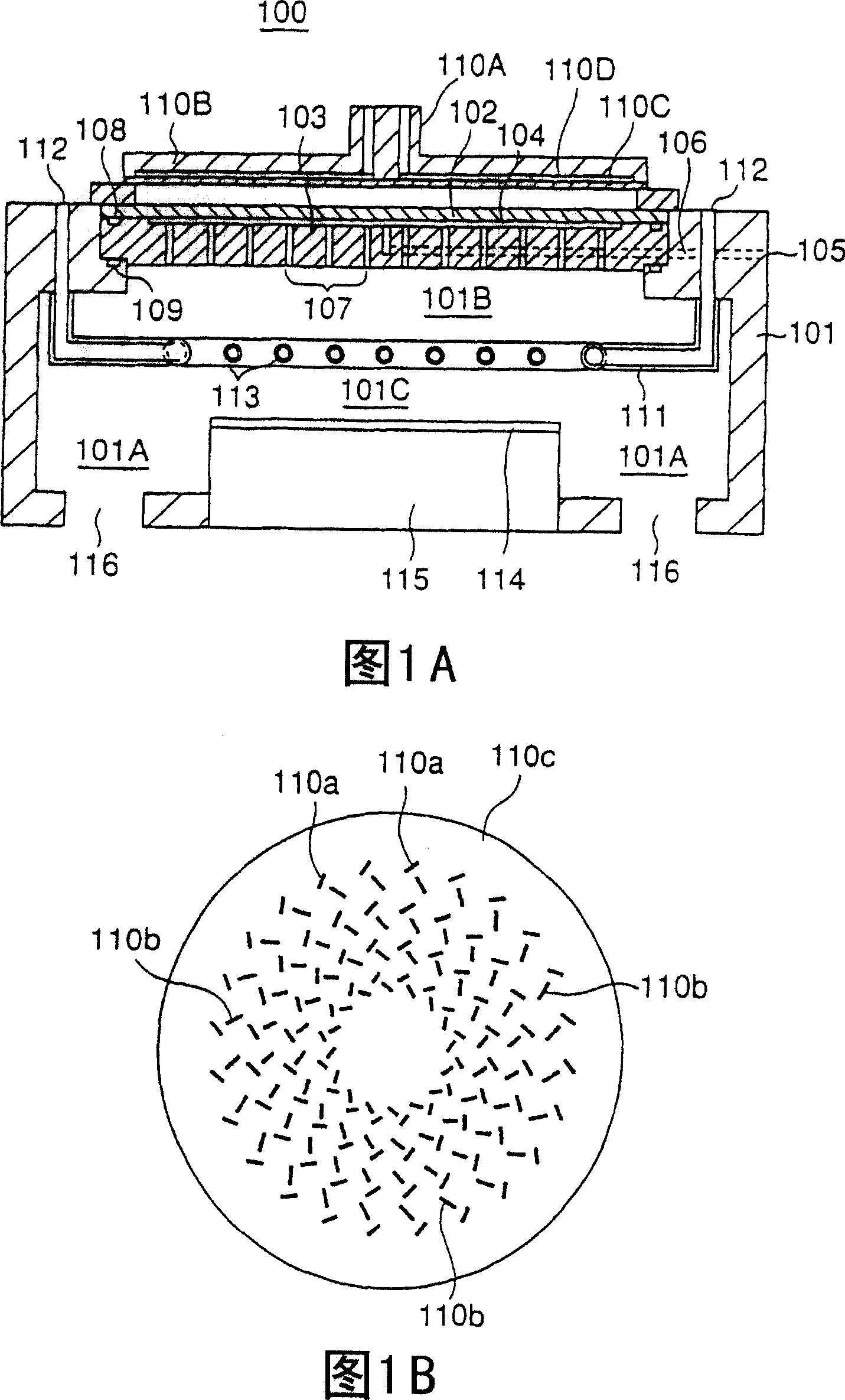
Plasma processing device
A plasma and processing device technology, applied in the field of plasma processing devices, can solve the problems of plasma density reduction, processing speed reduction, damage and the like
- Summary
- Abstract
- Description
- Claims
- Application Information
AI Technical Summary
Problems solved by technology
Method used
Image

Examples
no. 1 example
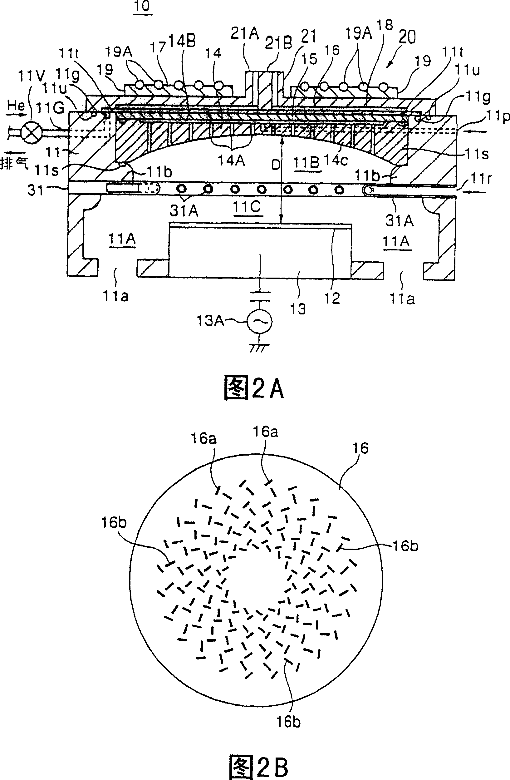
[0041] 2A and 2B are schematic structural diagrams of a microwave plasma processing apparatus 10 according to a first embodiment of the present invention.
[0042] Referring to FIG. 2A, the microwave plasma processing apparatus 10 includes a processing container 11 and a support table 13, the support table 13 is arranged in the processing container 11, and supports the processed substrate 12 by an electrostatic chuck, and the support table 13 Preferably made of AlN or Al formed by hot isostatic pressing (HIP) 2 o 3 In the space 11A surrounding the support table 13 of the processing container 11, at least two , It is preferable to form the exhaust ports 11a at three or more positions. The processing container 11 is exhausted and decompressed through the exhaust port 11a by screw pumps with different inclinations and inclinations.
[0043] The processing container 11 is preferably made of austenitic stainless steel containing Al, and a protective film composed of alumina is f...
no. 2 example
[0067] FIG. 5 is a schematic structural diagram of a plasma processing apparatus 10A according to a second embodiment of the present invention. In FIG. 5 , the same reference numerals are assigned to the previously explained parts, and their descriptions are omitted.
[0068] Referring to FIG. 5, the plasma processing apparatus 10A has a similar structure to the plasma processing apparatus 10, and the distance D between the substrate to be processed 12 and the spray disk 14 is outward in the radial direction of the spray disk 14. However, the processing gas supply part 13 is eliminated in the plasma processing apparatus 10A.
[0069] In the plasma processing apparatus 10B of the above structure, since the lower layer spray plate 31 is omitted, it is not possible to supply processing gas other than the plasma gas for film formation or etching treatment, but by supplying from the spray plate 14 Supplying oxidizing gas or nitriding gas simultaneously with plasma gas can form oxi...
no. 3 example
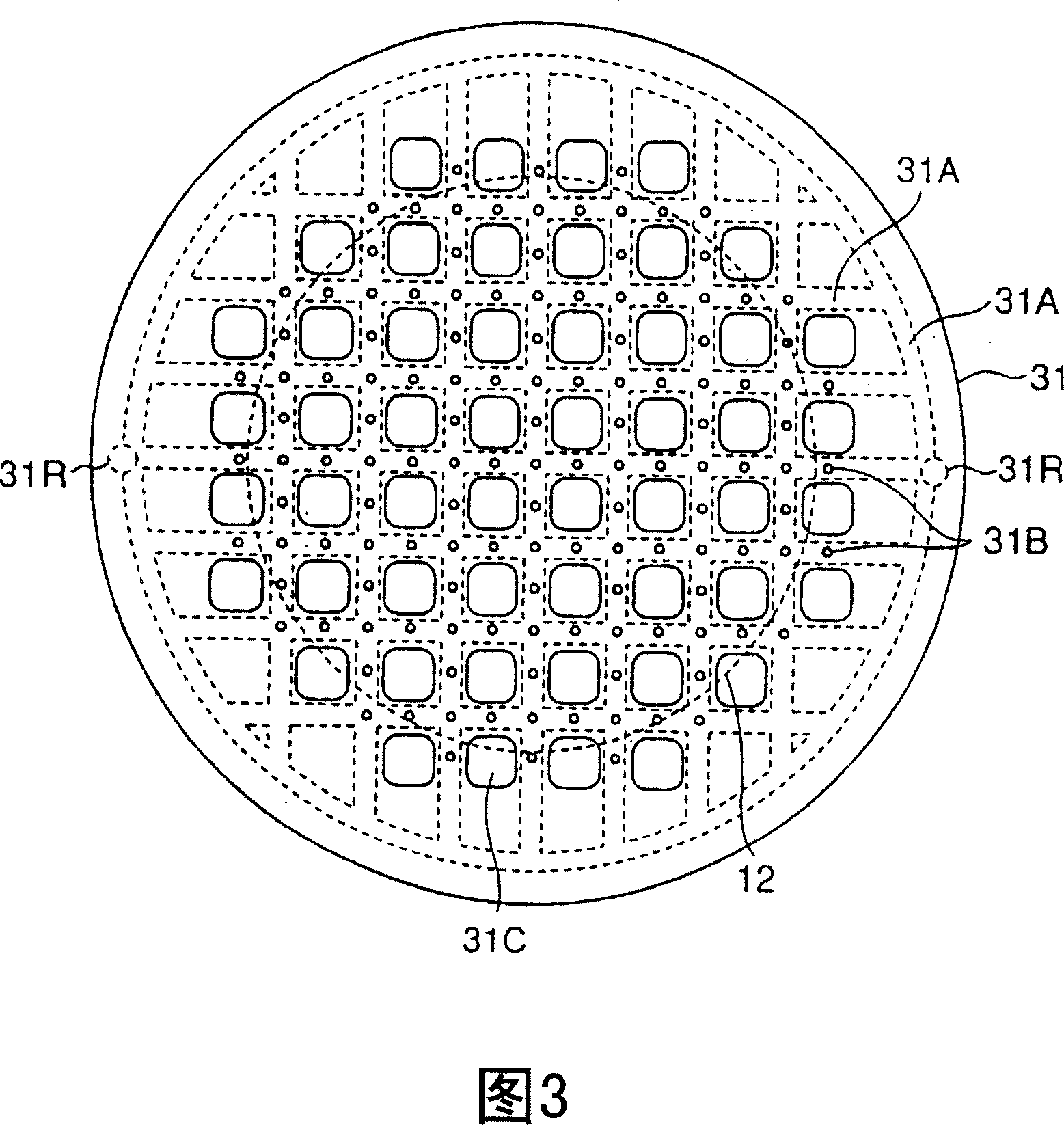
[0074] FIG. 6 is a schematic structural diagram of a plasma processing apparatus 10B according to a third embodiment of the present invention. However, in FIG. 6 , the same reference numerals are assigned to the previously described parts, and their descriptions are omitted.
[0075] Referring to FIG. 6 , in this embodiment, instead of the spray plate 14 , a spray plate 14 made of porous ceramic such as sintered alumina is used.
[0076] Although the nozzle opening portion 14A of the spray plate 14 in the spray plate 14P is not formed in the spray plate 14P, the plasma gas supply passages 14C and 14B connected to the plasma gas supply port 11P are formed, so that the supplied plasma The gas is uniformly discharged from the plasma gas channel 14B to the space 11B through the air holes in the porous medium spray plate 14 .
[0077] In this embodiment, the lower surface of the spray plate 14P forms an axisymmetric concave surface, and the distance D between the lower surface and...
PUM
| Property | Measurement | Unit |
|---|---|---|
| porosity | aaaaa | aaaaa |
Abstract
Description
Claims
Application Information