Pixel structure of thin film transistor liquid crystal display

A technology of thin film transistor and liquid crystal display, applied in the field of pixel structure

Inactive Publication Date: 2007-08-15
WINTEK CORP
View PDF0 Cites 27 Cited by
  • Summary
  • Abstract
  • Description
  • Claims
  • Application Information

AI Technical Summary

Problems solved by technology

Due to the structure designed in Figure 2, although it has a higher aperture ratio compared with the prior art in Figure 1, this pixel design must provide a ce

Method used


Image

  • Pixel structure of thin film transistor liquid crystal display
  • Pixel structure of thin film transistor liquid crystal display
  • Pixel structure of thin film transistor liquid crystal display

Examples


Embodiment Construction

[0044] Relevant technical contents and detailed description of the present invention are as follows in conjunction with accompanying drawing now:

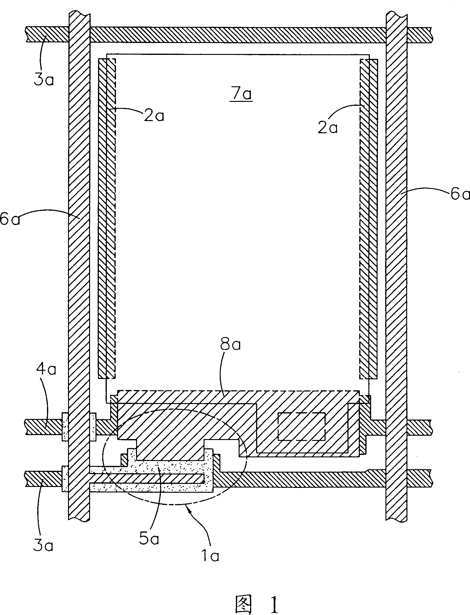
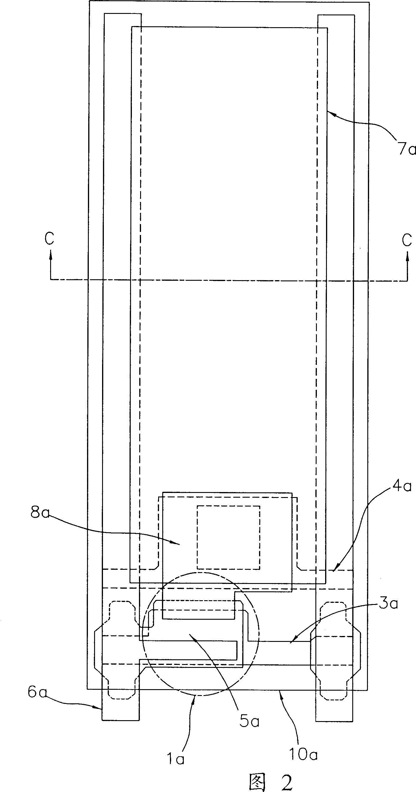
[0045] 4-19 are the structure of an embodiment of the pixel manufacturing process of the liquid crystal display of the present invention. The pixel structure of the thin film transistor liquid crystal display of the present invention is mainly used to increase the aperture ratio of the pixel, so as to increase the brightness, improve the display quality of the panel, and enhance product competitiveness.

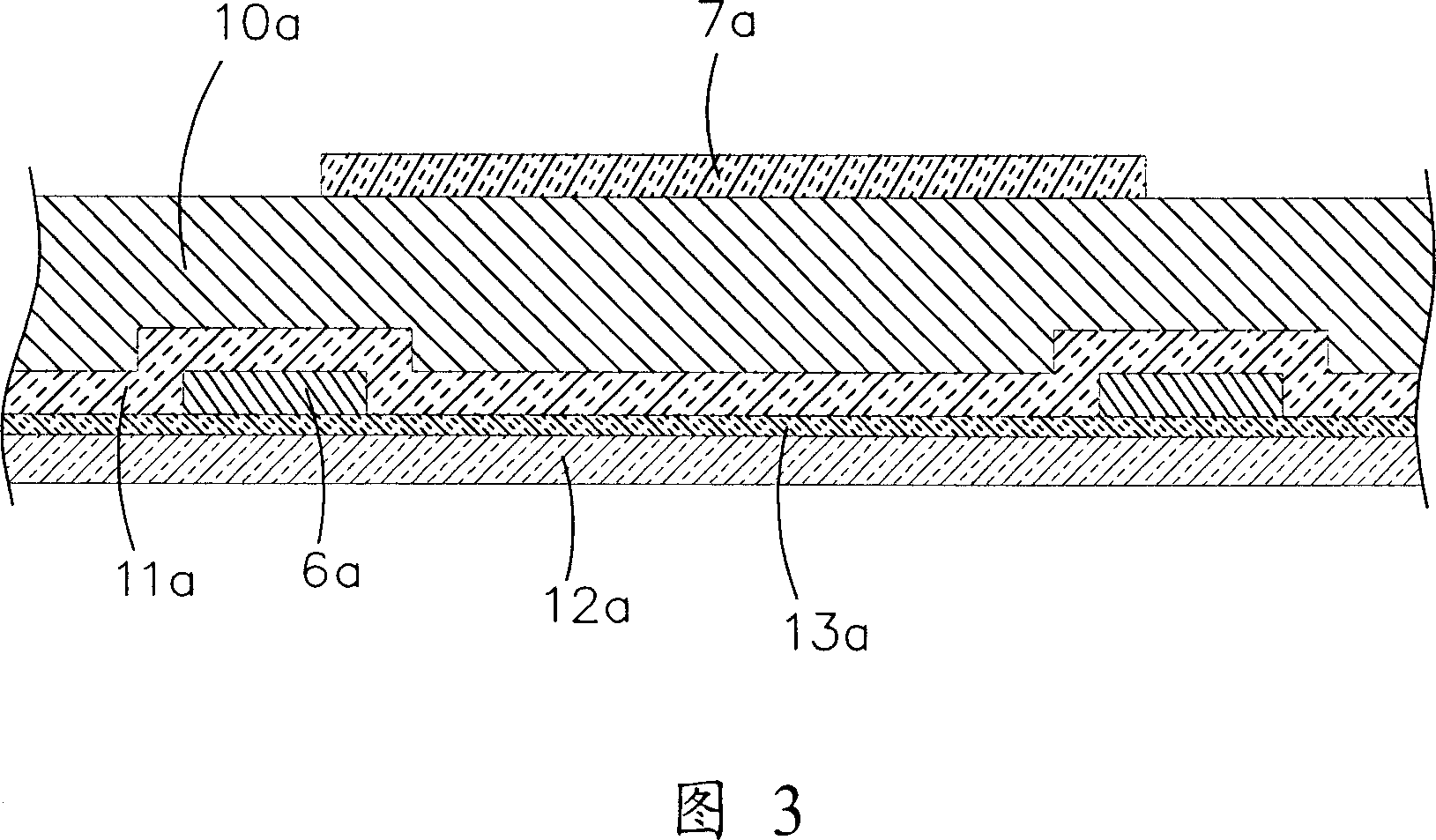
[0046] The pixel structure of the thin film transistor liquid crystal display of the present invention includes: a TFT structure 9, a scanning signal line 11 formed by a first conductive metal layer, an active area 10, a data signal line 3 formed by a second conductive metal layer, and a second conductive metal layer. Three conductive layers-common electrode 6, transparent conductive layer-pixel electrode 101 and second insulating...


PUM


Abstract

This invention relates to one film transistor LCD pixel structure, which uses three layers of metal layer design to make the data signal line and common electrode set with organic insulation layer to lower register capacitor; the common electrode and pixel electrode are set with passive layer as needed story capacitor for high open rate design.

Description

technical field [0001] The invention relates to a liquid crystal display, in particular to a pixel structure of a thin film transistor liquid crystal display. Background technique [0002] Liquid crystal display (Liquid Crystal Display; LCD) is widely used because of its advantages of low radiation and small size, and thin film transistor liquid crystal display (Thin Film Transistor LCD; TFT LCD) because of its contrast and viewing angle characteristics, It is still the mainstream display in the market. [0003] Since the liquid crystal material itself does not emit light, the light source of the TFT LCD comes from the backlight source. The backlight source passes through the layers of the TFT LCD such as polarizers, color filters and other materials, and the actual display brightness is only about that of the original light source. 10% or so. For the problem of insufficient display brightness, if the brightness of the backlight module is increased, although the brightness...

Claims


Application Information

Patent Timeline
IPC IPC(8): G02F1/136G02F1/133H01L21/00
Inventor 蔡哲福周怡伶王文俊
Owner WINTEK CORP
Why Eureka
Try Eureka