Polymer electrolytic thin film transistor
A technology of thin film transistors and electrolyte films, which is applied to electric solid devices, circuits, electrical components, etc., can solve the problems of increasing device area and limiting application scope, and achieve the effect of improving output current, broad application prospects and reducing operating voltage.
- Summary
- Abstract
- Description
- Claims
- Application Information
AI Technical Summary
Problems solved by technology
Method used
Image

Examples
Embodiment 1
[0025] Select poly[9,9-dioctylfluorene-9,9-(bis(3'-(N,N-dimethyl)-N-ethylammonium)propyl)fluorene]dibromide and 4,7- The polymer electrolyte (PFNBr-DBT) of bis(N-methylpyrrole)-2,1,3-phenylthiodiazo (DBT) was used to prepare thin film transistors according to the above steps.
[0026] Poly[9,9-dioctylfluorene-9,9-(bis(3'-(N,N-dimethyl)-N-ethylammonium)propyl)fluorene]dibromide and 4,7-di The chemical structural formula of the polymer electrolyte of (N-methylpyrrole)-2,1,3-phenylthiodiazo (DBT) is
[0027]
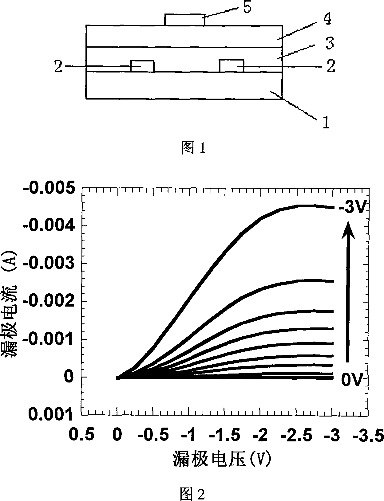
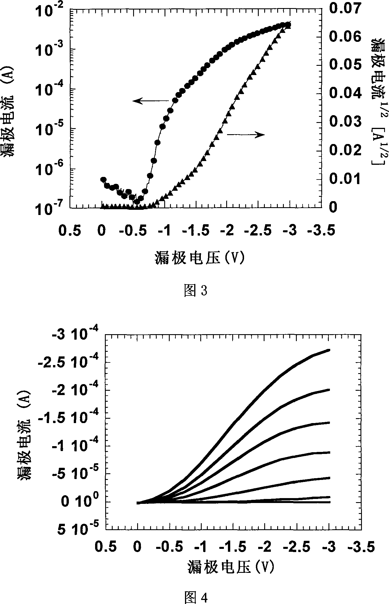
[0028] Figure 2 and Figure 3 show the output characteristic curve and transfer characteristic curve of the thin film transistor using PFNBr-DBT as the polymer electrolyte layer respectively. Figure 2 shows that the thin film transistors prepared by this method have typical saturation current output characteristics, and the saturation current increases as the gate voltage increases negatively, indicating that the carrier is a hole transport characteristic; Figure 3 shows...
Embodiment 2
[0032] Select poly[9,9-dioctylfluorene-9,9-(bis(3'-(N,N-dimethyl)-N-ethylammonium)propyl)fluorene]dibromide (PFNBr) polymer Electrolyte, prepare thin film transistor (condition is the same as embodiment 1).
[0033] The chemical structural formula of poly[9,9-dioctylfluorene-9,9-(bis(3'-(N,N-dimethyl)-N-ethylammonium)propyl)fluorene]dibromide is
[0034]
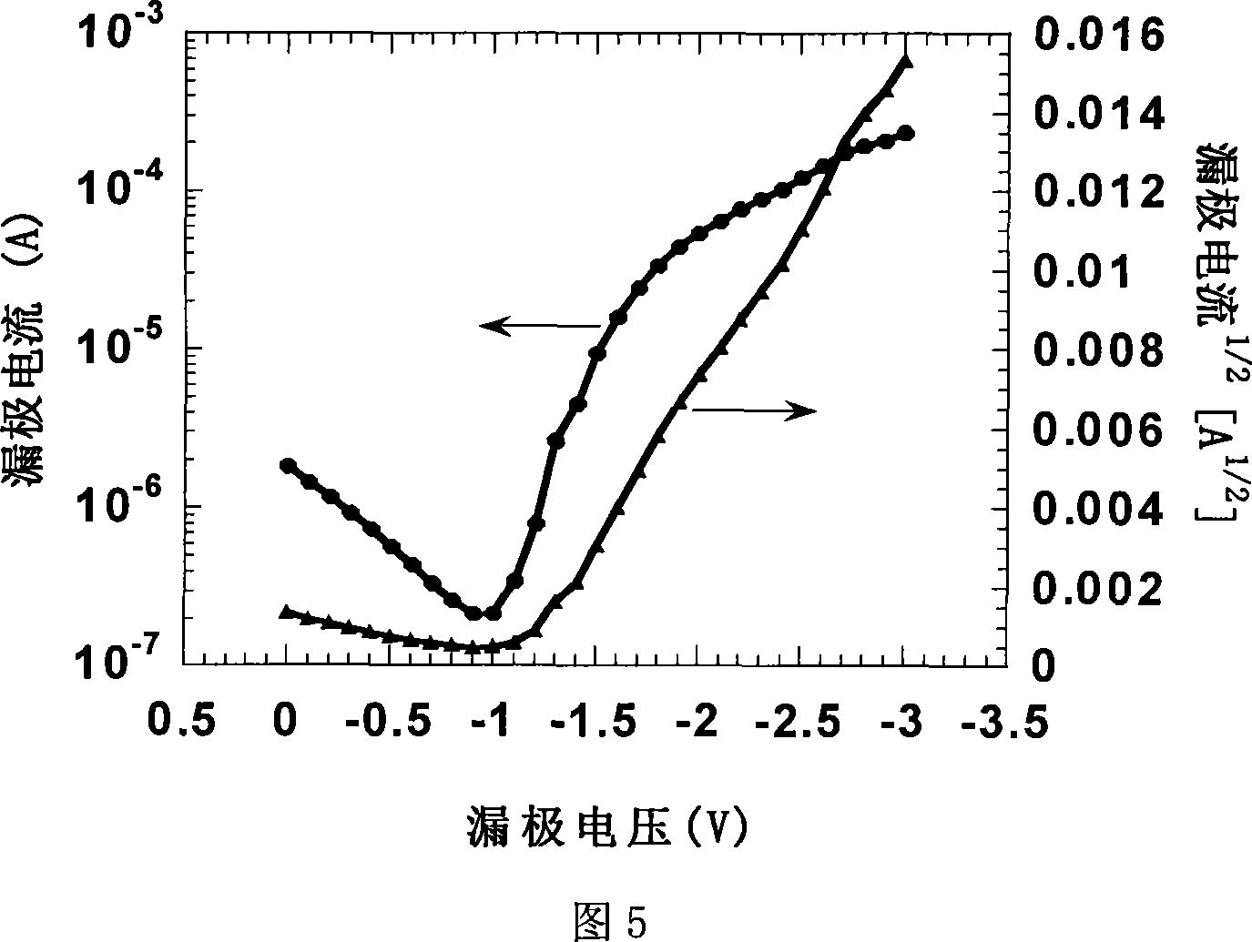
[0035] Figure 4 and Figure 5 respectively show the output characteristic curve and transfer characteristic curve of the thin film transistor using PFNBr as the polyelectrolyte layer. The output current tends to be saturated, and the threshold voltage of the transistor is about -1.2V, which is a hole carrier transport characteristic. When the gate bias voltage is equal to -3V, the output current reaches 0.3mA, and the calculated mobility is about 0.1cm 2 / Vs. It can be seen that the output current and mobility are related to the chemical structure of the electrolyte insulating layer.
PUM
 Abstract
Description
Claims
Application Information