Device and method for compensating MOS device grid leakage current

A gate leakage current, MOS device technology, applied in instruments, adjusting electrical variables, control/regulating systems, etc., to achieve the effects of reducing jitter, reducing circuit area, and improving working conditions

Inactive Publication Date: 2007-08-29
WUXI ZGMICRO ELECTRONICS CO LTD
View PDF0 Cites 14 Cited by
  • Summary
  • Abstract
  • Description
  • Claims
  • Application Information

AI Technical Summary

Problems solved by technology

[0007] The present invention provides a device and method for compensating the gate leakage current of deep submicron MOS devices to solve the problem of c

Method used


Image

  • Device and method for compensating MOS device grid leakage current
  • Device and method for compensating MOS device grid leakage current
  • Device and method for compensating MOS device grid leakage current

Examples


Embodiment 1

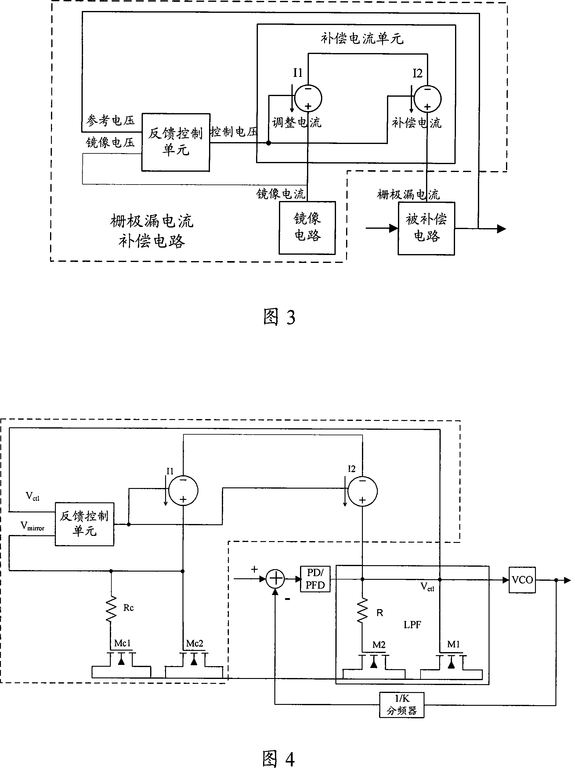
[0041] Please refer to FIG. 3 , which is a schematic structural diagram of a gate leakage current compensation device in an embodiment of the present invention, which mainly includes: a mirror circuit, a compensation current unit and a feedback control unit.

[0042] Among them, the mirror circuit is used to output the mirror voltage to the feedback control unit to generate the mirror current. The ratio of the gate leakage current of the compensated circuit to the mirror current is called the mirror ratio parameter. By setting the circuit of the compensated circuit and the mirror circuit The parameter can obtain the determined mirror ratio parameter; the structure of the mirror circuit corresponds to the circuit to be compensated to form its mirror image;

[0043] The compensation current unit is a unit that outputs a stable current under the control of the input control voltage, including two voltage-controlled current sources, one voltage-controlled current source is used to ...

Embodiment 2

[0055] Please refer to FIG. 4 , which is a specific embodiment of the present invention, which is a circuit diagram of a MOS device gate leakage current compensation device applied to a PLL circuit.

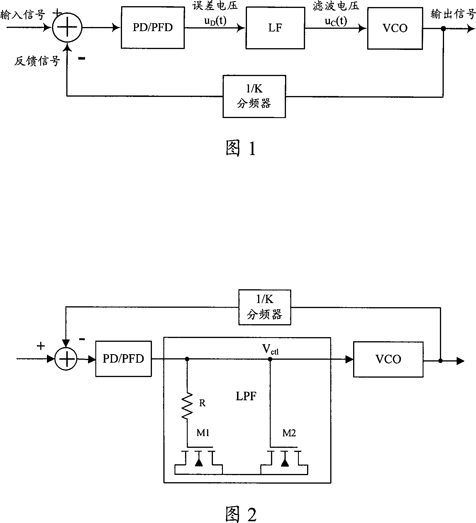
[0056] In the figure, PD or PFD, VCO, LPF and 1 / K frequency divider are all part of the conventional PLL circuit. The LPF is composed of a resistor R and NMOS transistors M1 and M2. M1 and M2 are thin gate MOS transistors with large capacitance per unit area. LPF output filter voltage V ctl is the VCO input voltage. Under deep sub-micron conditions, due to the tunneling effect, the MOS tube will generate a gate leakage current, which will affect the stability of the filter voltage in the PLL circuit and bring large jitter, which will seriously affect the PLL circuit. working status.

[0057] In this embodiment, the circuit to be compensated is the LPF, and a MOS device gate leakage current compensation circuit is added in the dotted line box to compensate the gate leakage curr...

Embodiment 3

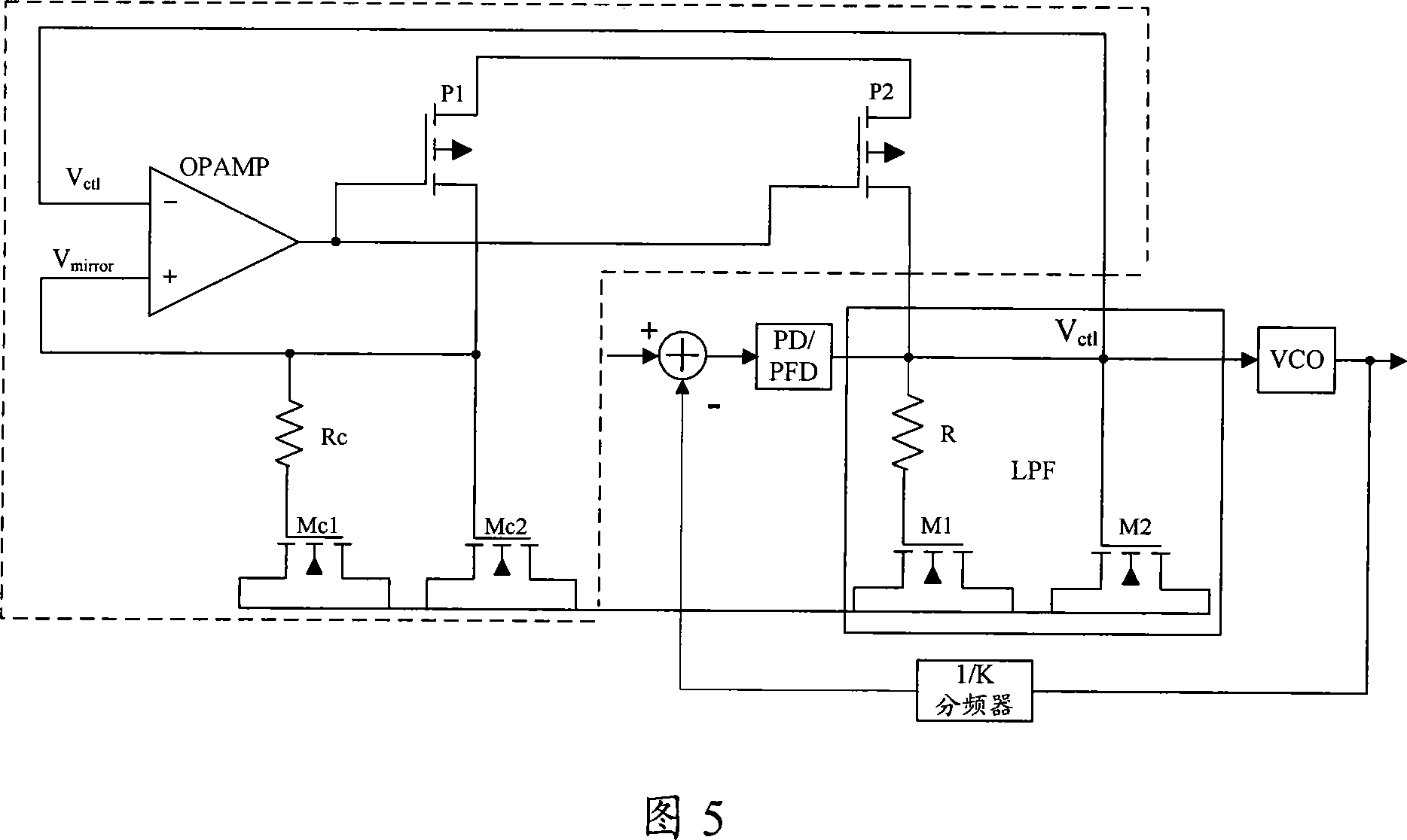
[0075] FIG. 5 shows another specific embodiment of the gate leakage current compensation circuit of the MOS device in the deep submicron PLL, which is a specific implementation of the second embodiment, wherein the feedback control unit is composed of an operational amplifier (Operational Amplifier, OPAMP) is implemented, and the voltage-controlled current source is implemented by a P-channel MOS (PMOS) tube. In this embodiment, the circuit to be compensated is an LPF, and the MOS device gate leakage current compensation circuit includes: a mirror circuit of the LPF, two PMOS transistors P1 and P2, and one OPAMP. The selection and connection methods of each device are described as follows:

[0076] The mirror circuit of LPF is composed of two NMOS transistors Mc1, Mc2 and a resistor Rc, the connection mode is corresponding to LPF; Mc1 is the mirror image of M1, the area is 1 / N of M1, and N is the mirror ratio parameter; Mc2 is the mirror image of M2 , the area is 1 / N of M2; R...


PUM


Abstract

The invention discloses a device and method for compensating gate leakage current of a MOS device, comprising: mirror circuit to output mirror voltage to a feedback control unit to generate mirror current, where the proportion of gate leakage current to mirror current is a mirror proportion parameter; compensation current unit to generate regulating current and compensation current to compensate the gate leakage current by the control of the control current outputted by a feedback control unit, where the proportion of compensation current to regulating current is a mirror proportion parameter; feedback control unit to respectively receive input voltage reference and mirror voltage coming from the junction of the mirror circuit and the compensation current unit and output control voltage to the compensation current unit according to the voltage reference and the mirror voltage, and regulate the regulating current of the compensation current unit according to the mirror current to make the regulating current equal to the mirror current.

Description

technical field [0001] The invention relates to analog integrated circuit technology, in particular to a device and method for compensating gate leakage current of a deep submicron MOS device. Background technique [0002] Phase Locked Loops (PLL) is a feedback control system in which the frequency of the output signal tracks the frequency of the input signal. When the frequency of the output signal is a fixed multiple of the frequency of the input signal, the output voltage and the input voltage maintain a fixed phase difference, so it is called a phase-locked loop, referred to as a phase-locked loop. [0003] The functional block diagram of the PLL circuit is shown in Figure 1. It is mainly composed of a phase comparator (Phase Detector, PD) or a phase frequency comparator (Phase frequency Detector, PFD), a loop filter (Loops Filter, LF) and a voltage-controlled oscillator. (Voltage Controlled Oscillator, VCO) consists of three parts. In the PLL circuit with relatively l...

Claims


Application Information

Patent Timeline
IPC IPC(8): G05F3/24G05F3/30
Inventor 赵纲张家川程宝洪
Owner WUXI ZGMICRO ELECTRONICS CO LTD
Why Eureka
Try Eureka