Chip-scale methods for packaging light emitting devices and chip-scale packaged light emitting devices

A light-emitting device and sealing layer technology, which is applied in semiconductor/solid-state device parts, semiconductor devices, electric solid-state devices, etc., can solve the problems of limiting the power level of LED chips that can be driven, huge packaging, and not suitable for miniaturized applications, etc.

Inactive Publication Date: 2007-09-05
CREE INC
View PDF33 Cites 58 Cited by
  • Summary
  • Abstract
  • Description
  • Claims
  • Application Information

AI Technical Summary

Problems solved by technology

The high cost of conventional packaging technologies may be a factor in making solid-state lighting cost per lumen high
Additionally, conventional packaging techniques can result in bulky packages that are not suitable for certain miniaturization applications such as cell phone backlighting
Conventional packaging technologies can also have poor thermal resistance characteristics, limiting the power levels at which the LED chip can be driven and placing constraints on LED placement for the system designer

Method used


Image

  • Chip-scale methods for packaging light emitting devices and chip-scale packaged light emitting devices
  • Chip-scale methods for packaging light emitting devices and chip-scale packaged light emitting devices
  • Chip-scale methods for packaging light emitting devices and chip-scale packaged light emitting devices

Examples


Embodiment Construction

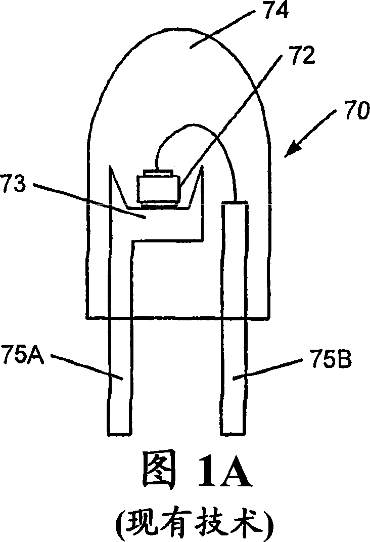
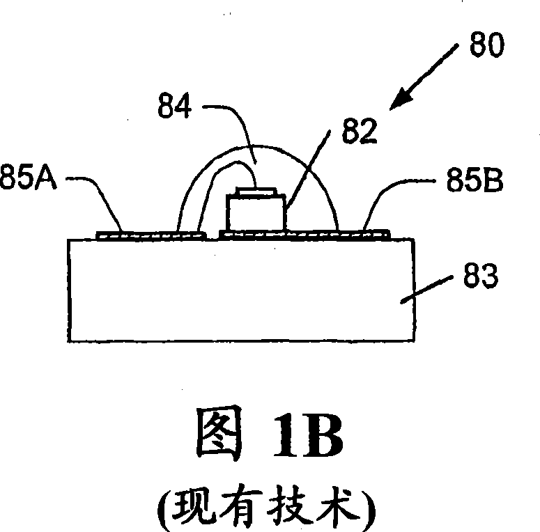
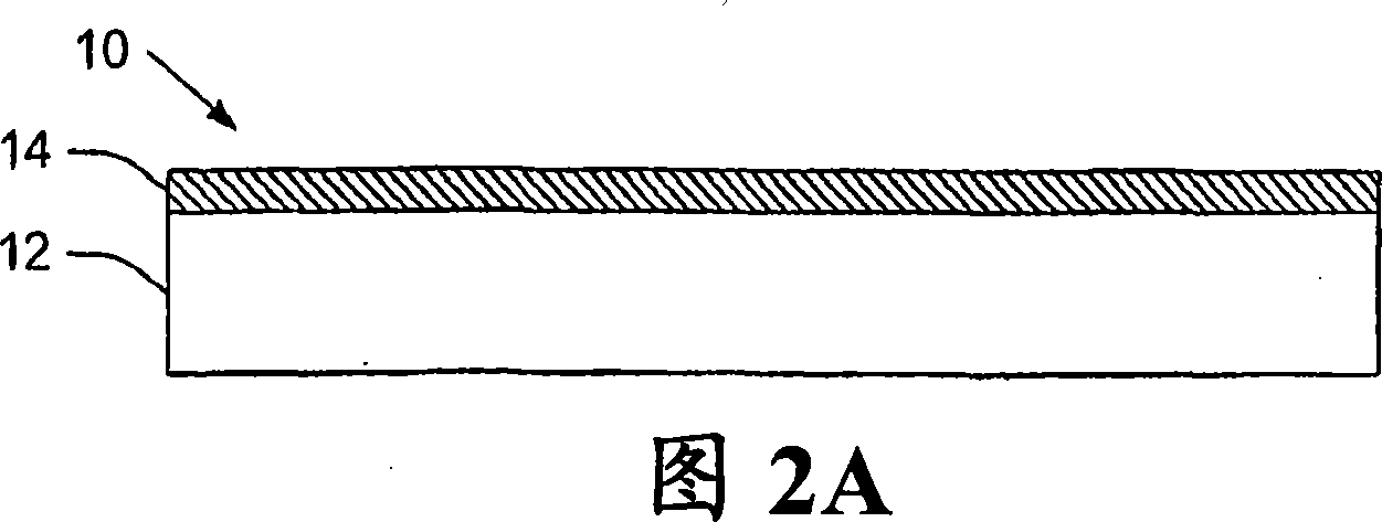
[0042] The present invention will now be described more fully hereinafter with reference to the accompanying drawings that show embodiments of the invention. The invention should not be construed as limited to the embodiments described herein; rather, these embodiments are provided so that this disclosure will be thorough and complete, and will fully convey the scope of the invention to those skilled in the art. Like numbers refer to like parts throughout the figures. Furthermore, the various layers and regions shown in the figures are shown schematically. Although the invention has been described with respect to semiconductor wafers and diced chips, such chips may be diced to any size, as will be understood by those skilled in the art. Accordingly, the invention is not limited to the relative sizes and spacing shown in the drawings. Additionally, certain features in the figures, such as layer thicknesses and feature dimensions, are shown in exaggerated size for clarity and ...


PUM


Abstract

A packaged light emitting device includes a carrier substrate having a top surface and a bottom surface, first and second conductive vias extending from the top surface of the substrate to the bottom surface of the substrate, and a bond pad on the top surface of the substrate in electrical contact with the first conductive via. A diode having first and second electrodes is mounted on the bond pad with the first electrode is in electrical contact with the bond pad. A passivation layer is formed on the diode, exposing the second electrode of the diode. A conductive trace is formed on the top surface of the carrier substrate in electrical contact with the second conductive via and the second electrode. The conductive trace is on and extends across the passivation layer to contact the second electrode. Methods of packaging light emitting devices include providing an epiwafer including a growth substrate and an epitaxial structure on the growth substrate, bonding a carrier substrate to the epitaxial structure of the epiwafer, forming a plurality of conductive vias through the carrier substrate, defining a plurality of isolated diodes in the epitaxial structure, and electrically connecting at least one conductive via to respective ones of the plurality of isolated diodes.

Description

[0001] CROSS REFERENCE TO PRIORITY STATEMENTS AND PROVISIONAL APPLICATIONS [0002] This application claims priority to U.S. Provisional Application No. 60 / 584,187, filed June 30, 2004, entitled "Chip Scale Packaging of Light Emitting Devices and Packaged Light Emitting Devices" rights and interests, the disclosure of this application is incorporated herein by reference as if fully set forth herein. technical field [0003] The present invention relates to a semiconductor device, and more particularly, to a packaged light emitting device and a method of packaging the light emitting device. Background technique [0004] Light-emitting diodes and laser diodes are well-known solid-state electronic devices that emit light when sufficient voltage is applied. Light emitting diodes and laser diodes may generally be referred to as light emitting devices (LEDs). Light emitting devices generally include p-n junctions formed in epitaxial layers grown on substrates such as...

Claims


Application Information

Patent Timeline
Patent Type & Authority Applications(China)
IPC IPC(8): H01L33/00H01L33/48H01L33/62
CPCH01L2224/16H01L2924/12041H01L2224/32245H01L33/62H01L2224/48247H01L33/486H01L2224/48091H01L2924/01004H01L23/481H01L2924/01078H01L2224/73265H01L24/48H01L2924/01079H01L2924/12035H01L2924/12042H01L2224/0508H01L2224/05568H01L2224/05023H01L2224/05001H01L2224/051H01L2224/056H01L2924/181H01L2924/00014H01L2924/00H01L2924/00012H01L2224/45099H01L2224/45015H01L2924/207
Inventor J·伊贝森B·凯勒P·帕里克
Owner CREE INC
Why Eureka
Try Eureka