Wide stress area silicon pressure sensor

A stress area and silicon pressure technology, applied in the field of silicon piezoresistive pressure sensor chips, can solve the problems of small area of ​​high stress area in the film, unable to provide manufacturing varistor area, affecting yield and other problems

Inactive Publication Date: 2007-09-12
TSINGHUA UNIV
View PDF0 Cites 19 Cited by
  • Summary
  • Abstract
  • Description
  • Claims
  • Application Information

AI Technical Summary

Problems solved by technology

[0006] However, with the improvement of sensor integration and the reduction of chip area, the area of ​​the film is getting smaller and smaller, and the area of ​​the high stress area in the film is also getting smaller and smaller, which cannot provide the area required...

Method used


Image

  • Wide stress area silicon pressure sensor
  • Wide stress area silicon pressure sensor
  • Wide stress area silicon pressure sensor

Examples


Embodiment Construction

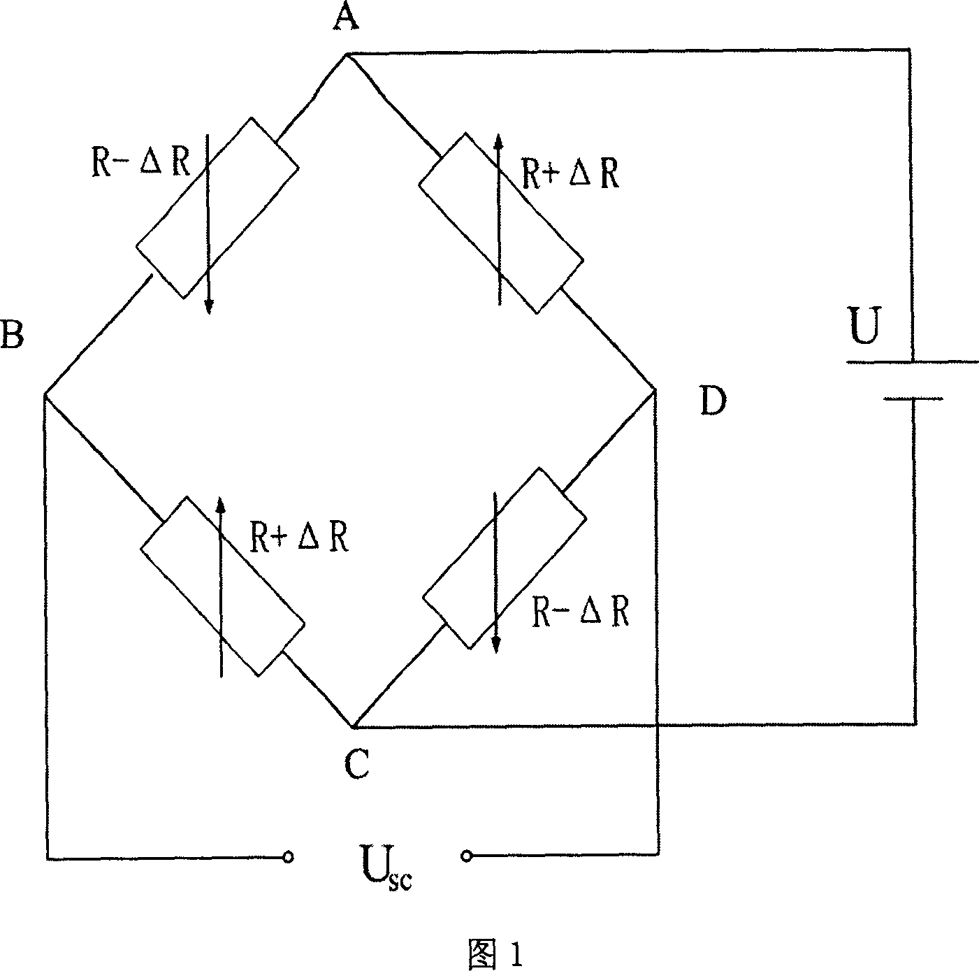
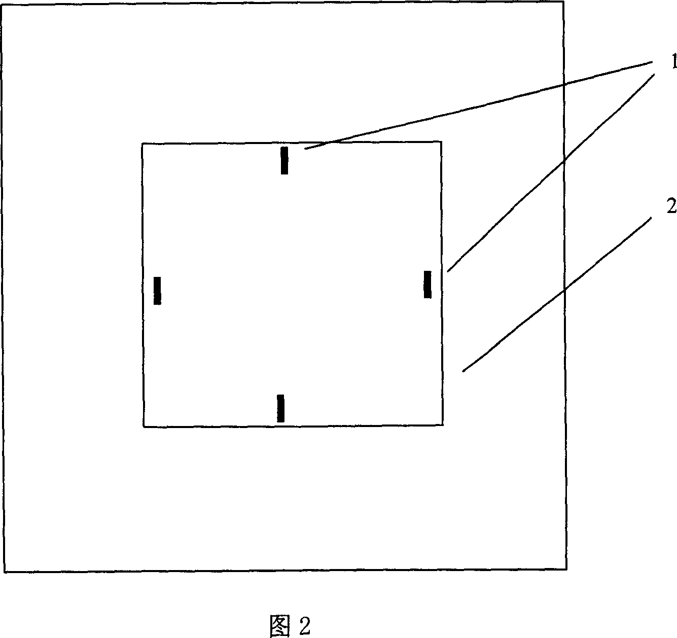
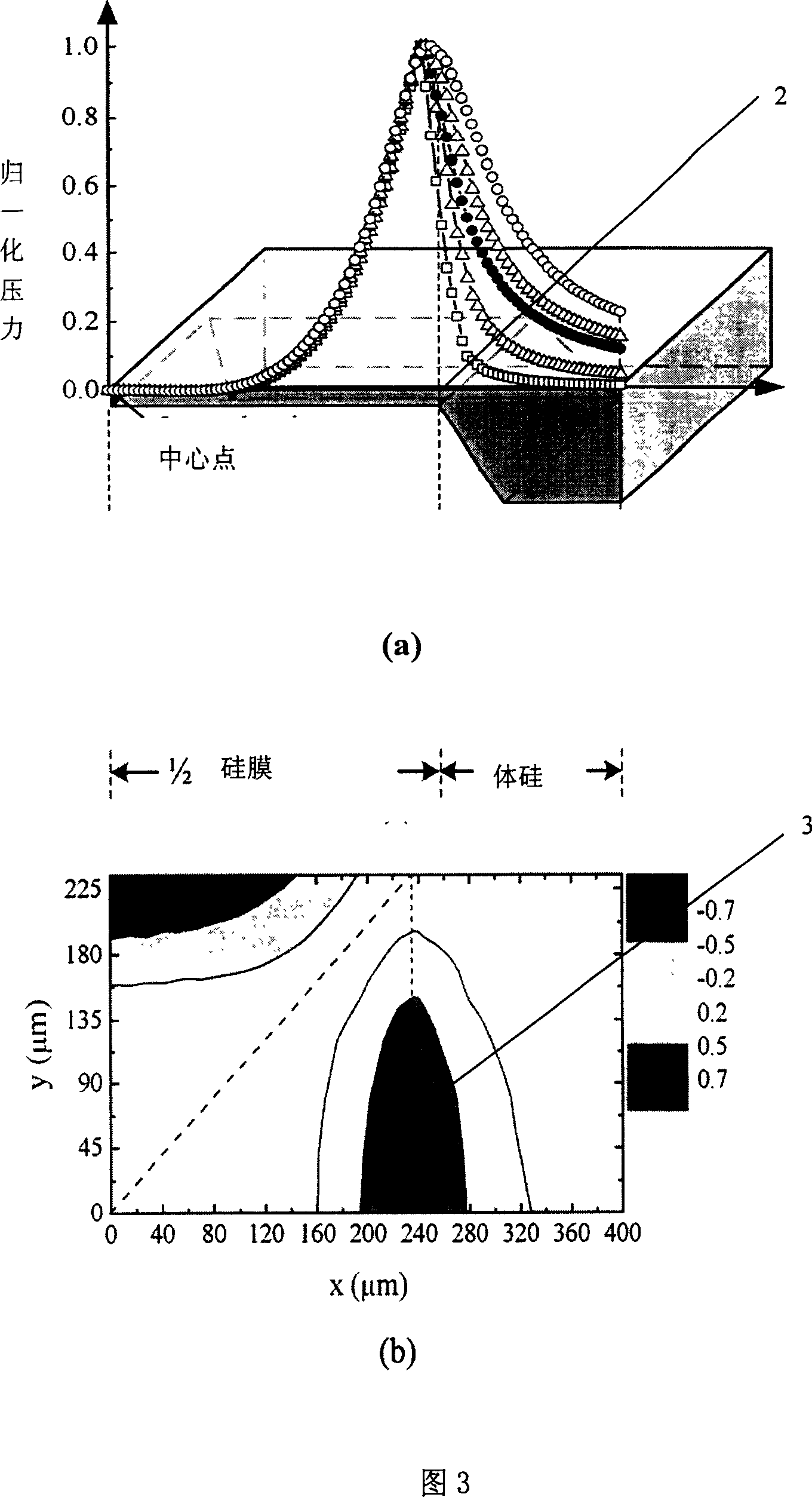
[0017] In order to overcome the improvement of sensor integration and the reduction of chip area, the area of ​​the film is getting smaller and smaller, and the area of ​​the high stress area in the film is also getting smaller and smaller, which cannot provide the area required for manufacturing piezoresistors, resulting in a serious reduction in the sensor. Sensitivity affects the yield; and if the method of narrowing the line is adopted, the difficulty of the process will be greatly increased, and the processing cost will be increased instead. A new type of high-sensitivity silicon pressure sensor chip structure in a large stress area, as shown in Figure 4.

[0018] The design has the following characteristics: first, the strained film adopts a large thickness-to-width ratio, which greatly expands the stress area outside the boundary; second, in order to make full use of the stress area, part of the resistance crosses the boundary of the film; third, the resistance uses diff...


PUM


Abstract

This invention belongs to semiconductor pressure sensor technosphere. The sensor includes pressure-sensing film that stressed zone stretched and supporting part around it. voltage dependent resistance lay in high-stress area that cross over pressure-sensing film, compose Wheatstone bridge, to convert pressure change to electrical signal; broken number of the described voltage dependent resistance perpendicular to pressure-sensing film's bound is greater than that parallel to pressure-sensing film bound, to meet shape of high stress region; resistance strip width of turnover section is greater than normal resistance strip width; processing ion implantation of high concentration at the same time to wane ohmic value of turnover section; the pressure-sensing film thickness-width ratio as far as possible large, to satisfy require of bound's high stress region width. The invention is at the condition of chip area reducing but line not reducing, utilize membrane outer region of high stress to increase stressed zone area, to advance sensor sensitivity and reduce numbers of rejects.

Description

technical field [0001] The invention belongs to the technical field of silicon piezoresistive pressure sensor chips. Background technique [0002] Because semiconductor sensors have the characteristics of small size, light weight, high precision, good temperature characteristics, and the manufacturing process is compatible with the planar process of semiconductor integrated circuits, they have been applied to a very wide range of fields-automotive, medical, aerospace, environment, etc. [0003] There are many kinds of pressure sensors, among which the simplest and easiest to mass-produce is the piezoresistive pressure sensor. The piezoresistive sensor has the advantages of high stability, high sensitivity, small zero output, and small temperature drift. [0004] The silicon piezoresistive pressure sensor has a silicon cup structure, including a pressure-sensitive film and its surrounding support parts, and four piezoresistors are fabricated in the maximum strain area within...

Claims


Application Information

Patent Timeline
IPC IPC(8): G01L1/18
Inventor 刘理天林惠旺张兆华任天令
Owner TSINGHUA UNIV
Why Eureka
Try Eureka