Image sensor

一种图像传感器、传感器的技术,应用在图像传感器领域,能够解决没有说明多个通道并行输出总和等问题,达到提高读出速度的效果

Active Publication Date: 2007-10-03
CANON KK
View PDF2 Cites 23 Cited by
  • Summary
  • Abstract
  • Description
  • Claims
  • Application Information

AI Technical Summary

Problems solved by technology

However, Japanese Patent Application Laid-Open No. 2005-130382 does not describe any concept of outputting the sum in parallel through multiple channels

Method used


Image

  • Image sensor
  • Image sensor
  • Image sensor

Examples


no. 1 example

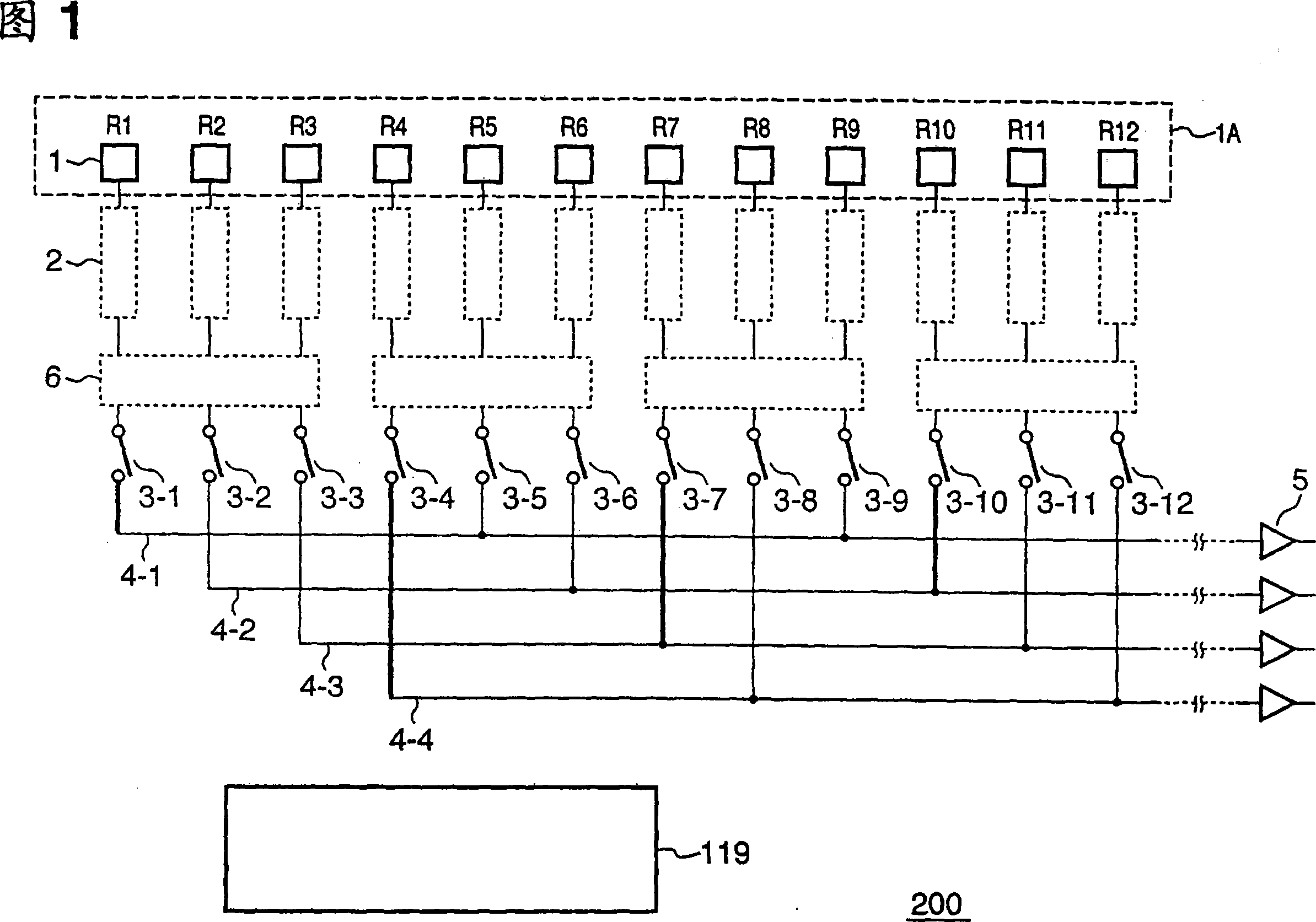
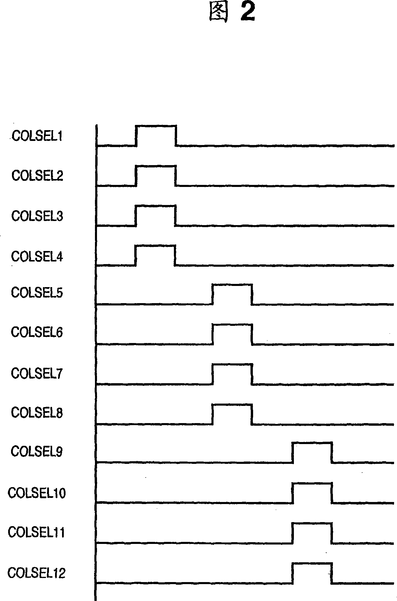
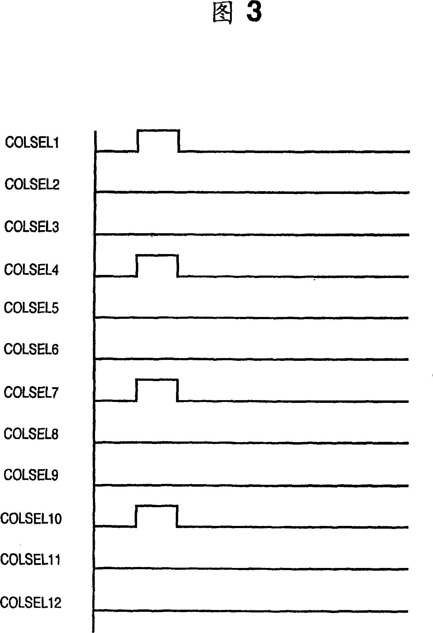
[0036] FIG. 1 is a circuit diagram showing a schematic configuration of an image sensor according to a first embodiment of the present invention. The image sensor 200 provides an all-pixel readout mode (second readout mode) in which pixel signals of all pixels are read out, and a low-resolution readout mode (first readout mode) in which one pixel signal is read out from each target readout area. model). As the low-resolution readout mode, the average readout mode will be exemplified below. Here, the average readout mode refers to a mode of reading out an average value of pixel signals of a plurality of pixels included in a target readout area.

[0037] The image sensor 200 includes a pixel array region 1A in which a plurality of pixels 1 are arranged. In the pixel array area 1A, the pixels 1 may be arranged to form a plurality of columns or one or more rows. FIG. 1 only shows the pixels R1-R12 in a row corresponding to the red filter. Each readout circuit 2 generates a pix...

no. 2 example

[0063] 7 is a circuit diagram showing a schematic configuration of an image sensor according to a second embodiment of the present invention. Color filters R, Gr, Gb, and B in the Bayer array are formed on the pixel 100, and the area sensor is composed of two-dimensionally arranged picture elements of 2×2 pixels.

[0064] FIG. 8 is an equivalent circuit diagram of the pixel 100 . The transfer pulses PTX, ie, PTX1, PTX2, . . . control the transfer switch 102 . The reset pulse PRES, ie PRES1, PRES2, . . . controls the reset switch 103 . Row selection pulses PSEL, PSEL1, PSEL2, . . . control the row selection switch 105 . The vertical scanning circuit 123 generates a transfer pulse PTX, a reset pulse PRES, and a row selection pulse PSEL.

[0065] The following describes the full pixel readout operation in the image sensor 300 shown in FIG. 7 with respect to the timing chart of FIG. 9 . The following description assumes that the set exposure time has elapsed and the photodiode...

no. 3 example

[0078] FIG. 12 is a block diagram showing a schematic configuration of an image sensor according to a preferred embodiment of the present invention. The camera 400 includes a solid-state image sensor 1004 exemplifying the image sensors according to the first and second embodiments.

[0079] The lens 1002 forms an optical image of the object on the image pickup plane of the image sensor 1004 . The outer surface of the lens 1002 is covered with a baffle 1001 which protects the lens 1002 and also acts as a main switch. The lens 1002 has a stop 1003 that adjusts the amount of light passing through the lens 1002 . The image pickup signal processing circuit 1005 performs various processing such as correction and clamping on the image pickup signal output from the image sensor 1004 through a plurality of channels. The A / D converter 1006 performs analog-to-digital conversion of the image pickup signal output from the image pickup signal processing circuit 1005 through a plurality of...


PUM


Abstract

An image sensor includes a plurality of operation circuits. The operation circuit operates pixel signals read out from a group of pixels included in a readout area to generate a pixel signal in the thinning readout mode. A plurality of column selecting switches are arranged between the output terminals of the plurality of operation circuits and a plurality of output channels. A control circuit controls the plurality of column selecting switches such that pixel signals the number of which is equal to the number of the plurality of output channels are output to the plurality of output channels in parallel in the thinning readout mode. The circuit arrangements, each included in the corresponding one of the plurality of operation circuits and each viewed from the corresponding one of the column selecting switches used in the thinning readout mode, are equivalent to each other.

Description

technical field [0001] The present invention relates to image sensors. Background technique [0002] Currently, image sensors of digital cameras have been significantly advanced, and a large number of pixels for higher resolution still images are being rapidly acquired. At the same time, an urgent problem is to increase the pixel signal readout speed in order to ensure the continuous shooting performance necessary for cameras. Japanese Patent Application Laid-Open No. 2005-286933 discloses a CCD image sensor that reads out pixel signals in parallel through a plurality of column shift registers, thereby increasing the readout speed. [0003] Digital cameras are capable of taking still images and even moving images. Digital cameras typically use one image sensor to capture still images and moving images. For still images, image sensors require high resolution, and for moving images, image sensors require high frame rates while reducing resolution to meet general moving imag...

Claims


Application Information

Patent Timeline
Patent Type & Authority Applications(China)
IPC IPC(8): H04N5/335H04N3/15H04N9/04H04N5/232H04N5/341H04N5/345H04N5/347H04N5/365H04N5/374H04N5/378
CPCH04N5/335H04N3/1568H04N5/23245H04N23/667H04N25/46H04N25/75H04N25/677H04N25/00
Inventor 樋山拓己高田英明波多野雄一朗有嶋优
Owner CANON KK
Why Eureka
Try Eureka