Image sensing device and camera

a sensing device and image technology, applied in the field of image sensing devices and cameras, can solve the problems of increased leakage current, high consumption power, disadvantages rather than advantages, etc., and achieve the effect of reducing the noise of 1/f in each pixel and high readout speed of signals

Inactive Publication Date: 2013-07-09
CANON KK
View PDF83 Cites 8 Cited by
  • Summary
  • Abstract
  • Description
  • Claims
  • Application Information

AI Technical Summary

Benefits of technology

[0006]The present invention has been made because of recognition of the aforementioned subjects, and attains, for example, both a reduction of 1 / f noise in each pixel and a high readout speed of a signal in an image sensing device.

Problems solved by technology

For this reason, a leak current may increase, and consumption power may become high.
The channel stop region arranged in the column selecting circuit not only increases an ON resistance but also disturbs miniaturization, resulting in disadvantages rather than advantages.
When a portion that especially requires a high-seed operation in a peripheral circuit (in particular, a MOS transistor of the column selecting circuit (also called a column decoder or horizontal scanning circuit)) uses the same structure as the amplifier MOS transistor of each pixel, an image sensing device having a sufficiently high readout speed cannot be obtained.

Method used


Image

  • Image sensing device and camera
  • Image sensing device and camera
  • Image sensing device and camera

Examples


Embodiment Construction

[0023]Embodiments of the present invention will be described hereinafter with reference to the accompanying drawings.

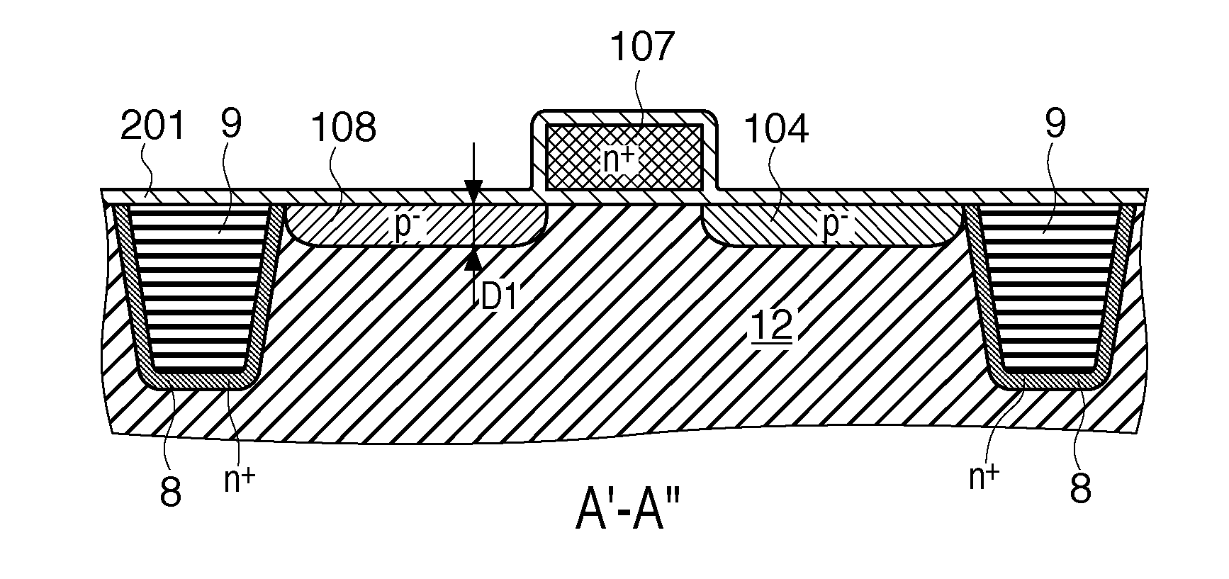
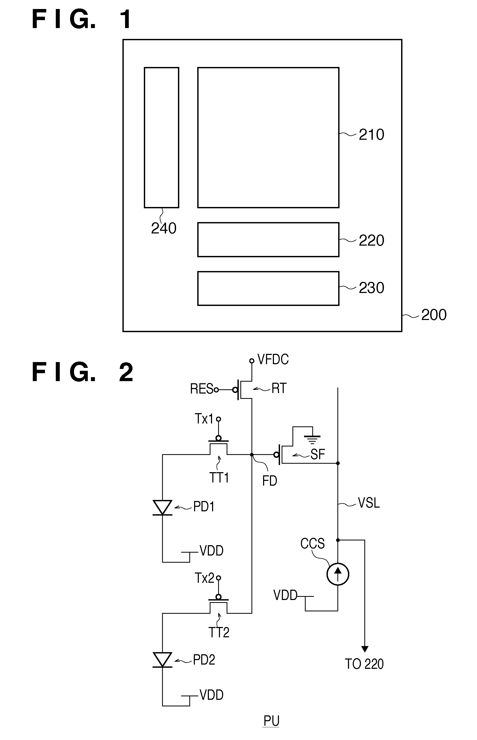
[0024]FIG. 1 is a schematic view showing the arrangement of an image sensing device 200 according to an embodiment of the present invention. The image sensing device 200 is formed on a semiconductor substrate, and can be called, for example, a solid-state image sensor, MOS image sensor, CMOS sensor, or the like.

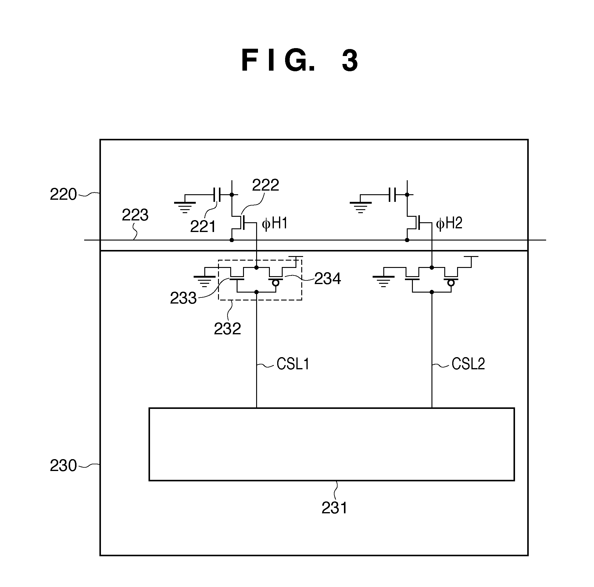
[0025]The image sensing device 200 according to the embodiment of the present invention includes a pixel array 210 in which pixels are two-dimensionally arranged to form a plurality of rows and a plurality of columns. The image sensing device 200 can also include a row selecting circuit 240 which selects a row in the pixel array 210, a column selecting circuit 230 which selects a column in the pixel array 210, and a readout circuit 220 which reads out a signal of the column selected by the column selecting circuit 230 in the pixel array 210. The row selecting c...


PUM

PropertyMeasurementUnit
channel width WCRaaaaaaaaaa
concentrationaaaaaaaaaa

Abstract

An image sensing device comprises a pixel array, and a peripheral circuit, a column selecting circuit, and a readout, wherein each pixel includes a photodiode, a floating diffusion, a transfer PMOS transistor to the floating diffusion, an amplifier PMOS transistor, and a reset PMOS transistor, the amplifier PMOS transistor has a gate which is formed by an n-type conductive pattern, and is isolated by a first element isolation region and an n-type impurity region which covers at least a lower portion of the first element isolation region, and each PMOS transistor included in the column selecting circuit has a gate which is formed by a p-type conductive pattern and is isolated by a second element isolation region, and an n-type impurity concentration in a region adjacent to a lower portion of the second element isolation region is lower than that in the n-type impurity region.

Description

TECHNICAL FIELD[0001]The present invention relates to an image sensing device and a camera.BACKGROUND ART[0002]As disclosed in Japanese Patent Laid-Open No. 2006-120679, 1 / f noise is reduced when the gate of an amplifier transistor included in each pixel of a MOS image sensor is formed to have a buried channel structure. As disclosed in the paragraph “0034” of Japanese Patent Laid-Open No. 2006-120679, as a method of forming the buried channel structure, when the amplifier transistor is a MOS transistor of a first conductivity type, its gate electrode is formed by polysilicon of a second conductivity type. As disclosed in the paragraph “0062” of Japanese Patent Laid-Open No. 2006-120679, a PMOS transistor can be used as the amplifier transistor in place of an NMOS transistor.[0003]Japanese Patent Laid-Open No. 2006-120679 has not examined about channel structures of transistors in a peripheral region as a region other than a pixel region. If that reference pursuits process simplific...

Claims


Application Information

Patent Timeline
Patent Type & Authority Patents(United States)
IPC IPC(8): H04N3/14H01L31/00H01L29/04H01L29/10H01J40/00C12Q1/68H04N5/335H01L27/146H04N5/357H04N5/361H04N5/369H04N5/374
CPCH01L27/14609H01L27/1463H01L27/14641H01L27/1464H01L27/14689H01L29/7833H01L27/146H04N25/00
Inventor WATANABE, TAKANORISHIMOTSUSA, MINEOICHIKAWA, TAKESHIIKEDA, HAJIMESEKINE, YASUHIROOHTANI, AKIRAKOJIMA, TAKESHI
Owner CANON KK
Why Eureka
Try Eureka