Supercharge Your Innovation With Domain-Expert AI Agents!

Semiconductor luminous device and luminous screen with thereof

A technology for light-emitting devices and semiconductors, which is applied to semiconductor devices, semiconductor devices of light-emitting elements, cooling/heating devices of lighting devices, etc., to achieve good cooling effects

Inactive Publication Date: 2010-11-03
诺克特龙控股有限公司
View PDF4 Cites 0 Cited by
  • Summary
  • Abstract
  • Description
  • Claims
  • Application Information

AI Technical Summary

Problems solved by technology

Therefore, in the known semiconductor light-emitting device, the light emitted to the rear half space is mostly or completely lost

Method used


Image

  • Semiconductor luminous device and luminous screen with thereof
  • Semiconductor luminous device and luminous screen with thereof
  • Semiconductor luminous device and luminous screen with thereof

Examples


Embodiment Construction

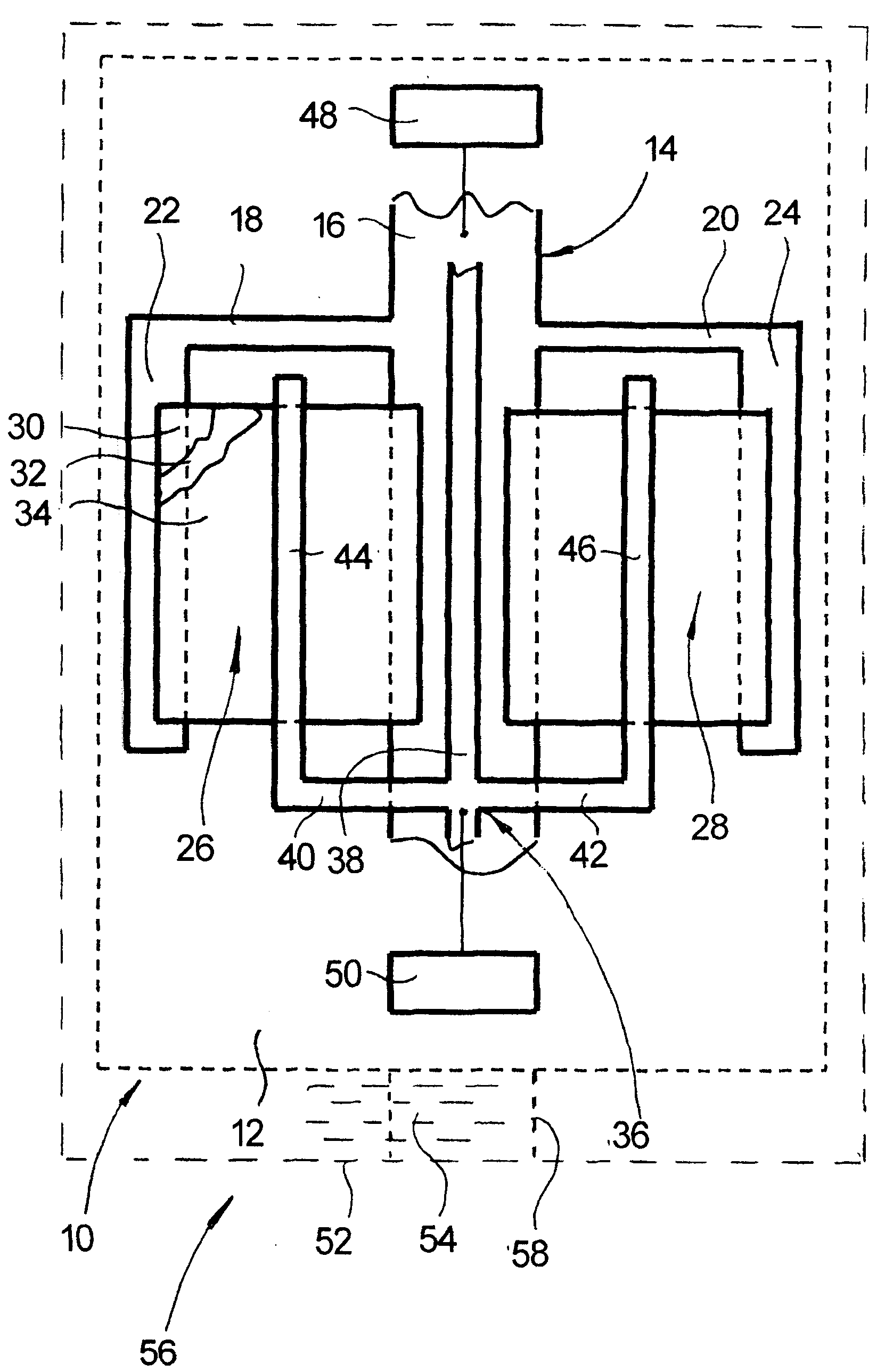
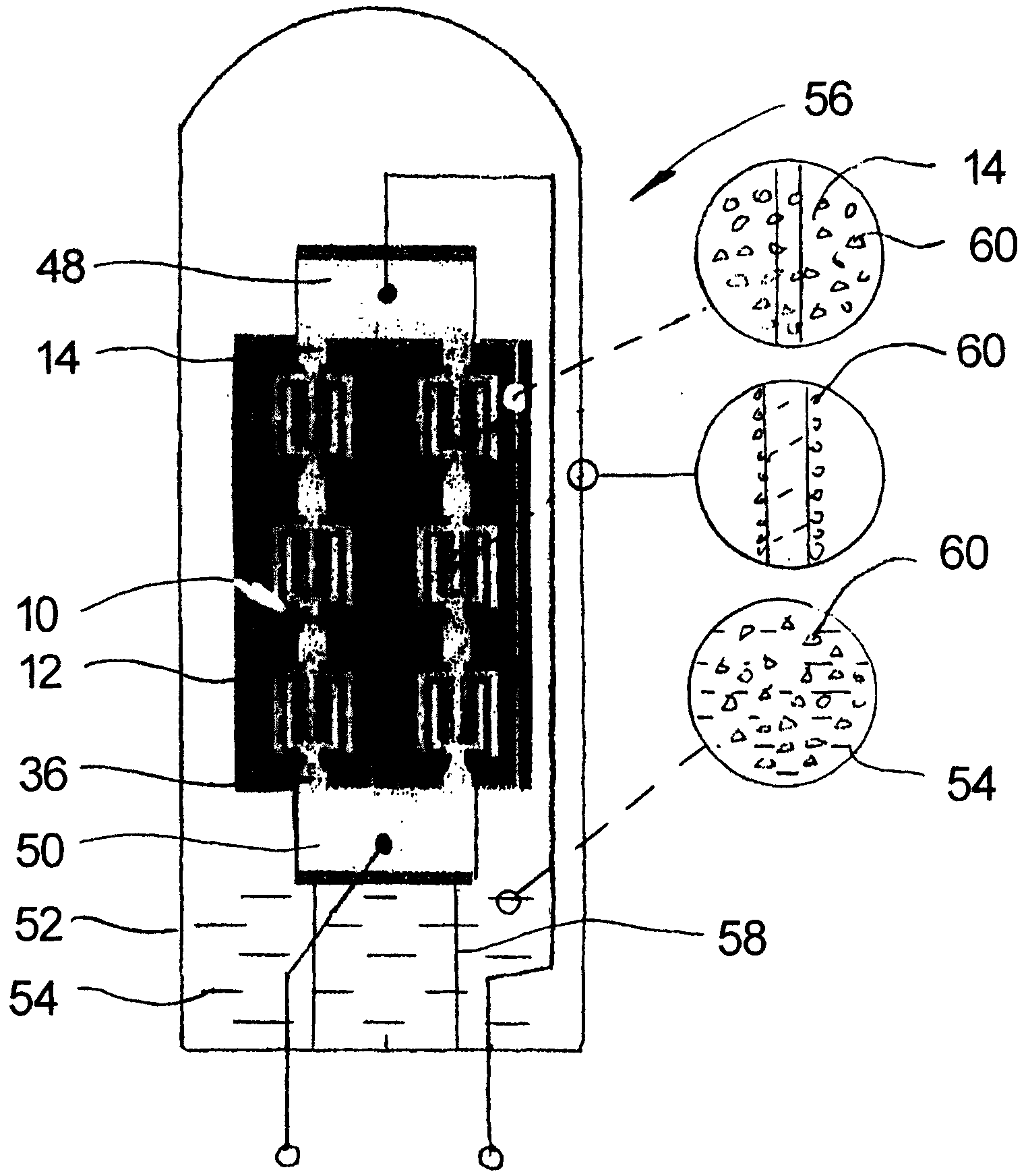
[0071] exist figure 1 In general, 10 represents a light-emitting element unit, which includes a corundum glass (Korundglas) (Al 2 o 3 glass) which is also marketed under the name sapphire glass. Such glasses are characterized by high mechanical strength, good insulating properties and good thermal properties. Base body 12 has a thickness of 300 to 400 μm in practice.

[0072] Arranged on the upper side of the base body 12 is a first electrode, generally designated 14 .

[0073] The electrode comprises a central connecting conductor line 16 , which supports via transverse arms 18 , 20 contact arms 22 , 24 running parallel to connecting conductor track 16 .

[0074] The two planar luminous elements 26 , 28 are laid on the connecting conductor track 16 and the contact arms 22 , 24 in such a way that they partially overlap the connecting conductor track and the contact arms in the transverse direction, as shown.

[0075] Each light-emitting element 26, 28 comprises three lay...


PUM

PropertyMeasurementUnit
thicknessaaaaaaaaaa
thicknessaaaaaaaaaa
thicknessaaaaaaaaaa

Abstract

The invention relates to a semiconductor-illuminating device, comprising at least one semiconductor-illuminating units (26, 28, 1016, 2016, 3016) which can illuminate on loading pressure and substrates (12, 1014, 2014, 3014) supporting the illuminating units. The light from the semiconductor-illuminating units (26, 28, 1016, 2016, 3016) can penetrate through the substrates (12, 1014, 2014, 3014).

Description

technical field [0001] The invention relates to a semiconductor luminous device having at least one semiconductor luminous element which emits light when a voltage is applied and a base body which supports the semiconductor luminous element and a luminous panel with such a semiconductor luminous device. Background technique [0002] Semiconductor light-emitting devices in the form of light-emitting diodes (LEDs) are known, in which a semiconductor crystal comprising a pn junction is supported by a light-tight substrate. [0003] Semiconductor light-emitting crystals emit light from the recombination of electrons and holes in all directions. The light emitted into the rear half of the space is thus largely or completely lost in known semiconductor light emitting devices. Contents of the invention [0004] The invention is intended to improve a semiconductor light-emitting arrangement having at least one semiconductor light-emitting element which emits light when an elec...

Claims


Application Information

Patent Timeline
Patent Type & Authority Patents(China)
IPC IPC(8): H01L33/00F21S4/00F21V29/00G02F1/13357H01L33/56H01L33/64
CPCH01L33/648H01L2224/49109H01L2224/48091H01L33/56F21K9/00F21S10/002F21K9/64H01L2224/48247H01L2224/48257H01L2224/8592H01L2924/181F21Y2115/10H01L2924/00014H01L2924/00012
Inventor G·迪亚曼蒂迪斯
Owner 诺克特龙控股有限公司
Features
  • R&D
  • Intellectual Property
  • Life Sciences
  • Materials
  • Tech Scout
  • Unparalleled Data Quality
  • Higher Quality Content
  • 60% Fewer Hallucinations
Learn More