
Voltage follower of small output resistance, large output amplitude

A technology of voltage follower and output resistance, which is applied in the direction of differential amplifiers, DC-coupled DC amplifiers, etc., and can solve the problems of small output resistance and voltage fluctuation of voltage followers

Inactive Publication Date: 2007-10-10
TSINGHUA UNIV
View PDF0 Cites 20 Cited by
  • Summary
  • Abstract
  • Description
  • Claims
  • Application Information

AI Technical Summary

Problems solved by technology

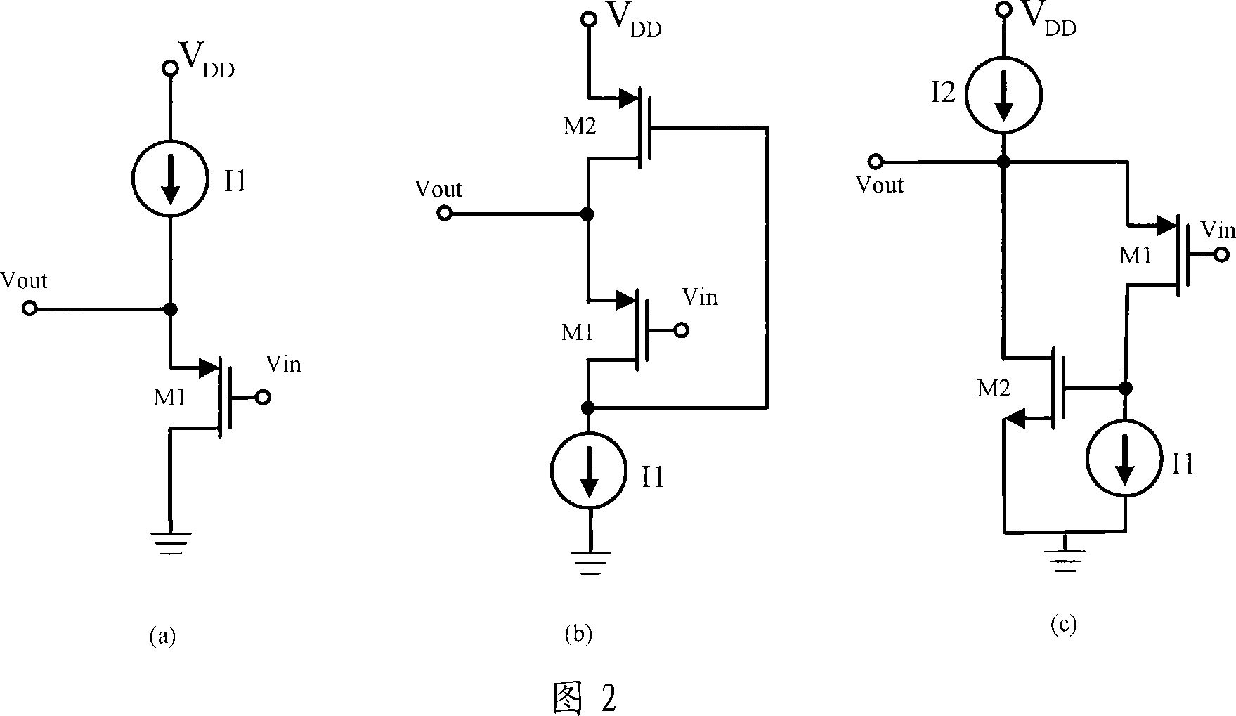
[0012] In addition, in some applications such as source-level attenuating transconductance amplifiers, the voltage follower needs to have a very small output resistance to achieve good linearity. The output resistance of the above two voltage followers cannot meet this requirement well.
In addition, because the drain of the above-mentioned voltage follower is very high impedance, it will bring a large voltage fluctuation at this point, so the channel modulation effect of the output transistor will be more obvious

Method used


Image

  • Voltage follower of small output resistance, large output amplitude
  • Voltage follower of small output resistance, large output amplitude

Examples


Embodiment Construction

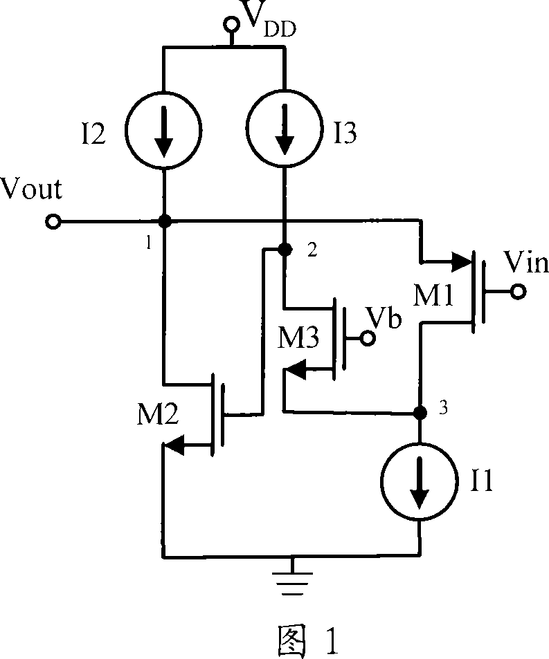
[0030] Technical solution of the present invention refers to Fig. 1. Figure 1 is a circuit structure diagram of a voltage follower with a small output resistance and a large output range.

[0031] The specific connection relationship of the entire voltage follower with small output resistance and large output amplitude is: the source of the M1 tube is connected to node 1, the drain is connected to node 3, and the gate is connected to the input signal Vin. M2 tube, M3 tube, current sink I1 and current source I3 form a feedback loop. Node 1 is externally connected to the output port Vout. The source of the M2 tube is connected to the ground, and the drain is connected to node 1. The gate is connected to node 2. The source of the M3 tube is connected to the node 3, the drain is connected to the node 2, the gate is connected to the bias voltage Vb, and the Vb voltage is provided by the bias circuit. One end of the current sink I1 is grounded and the other end is connected to n...


PUM


Abstract

Characters of the voltage follower are that a feedback loop is composed of one PMOS input tube M1, first current source I2, two NMOS tubes M2 and M3, a current sink I1, and second current source I3. The feedback loop reduces output resistance, and increases output amplitude of the voltage follower remarkably. At same time, drain electrode of the input tube of the voltage follower becomes a node with low impedance so as to make fluctuation of drain voltage of the input tube become smaller as well as reduce effect of channel modulation of input tube. Advantages are: small output resistance, large output amplitude, high linearity, and suitable to be operated at low voltage.

Description

technical field [0001] The invention belongs to the design of ultra-large-scale integrated circuits in the field of microelectronics and solid-state electronics, and relates to a new type of voltage follower circuit, which can be widely used in source attenuation structure transconductance amplifiers and tube-based transconductance amplifiers operating in the linear region, etc. circuit design. Background technique [0002] As the feature size of the CMOS process begins to enter the nanometer level, analog circuits need to work at lower and lower power supply voltages to meet the requirements of the process. But the threshold voltage of the transistor (V T ) and saturation voltage (V Dsat ) does not decrease linearly with the supply voltage synchronously. These factors severely limit the voltage amplitude of analog circuits at low supply voltages. In the published literature, a variety of methods have been proposed to allow analog circuits to operate at low voltages whil...

Claims


Application Information

Patent Timeline
IPC IPC(8): H03F3/45
Inventor 孔耀晖杨华中
Owner TSINGHUA UNIV
Learn More