
Chip data output signal protection method and its circuit

A technology for outputting signals and chips, used in electrical digital data processing, protection of internal/peripheral computer components, instruments, etc., can solve problems such as production difficulties, increased chip costs, and inability to protect codes, achieving no special process requirements and low cost. Effect

Inactive Publication Date: 2007-10-17
SOUTHEAST UNIV
View PDF0 Cites 4 Cited by
  • Summary
  • Abstract
  • Description
  • Claims
  • Application Information

AI Technical Summary

Problems solved by technology

[0002] Many embedded SOCs (System On Chip) are embedded with FLASH flash memory to reduce chip pins. The JTAG interface is a general debugging interface, which must be reserved for each SOC. Through the JTAG interface, data can be written to the embedded FLASH flash memory. , can also read out the data, so the code cannot be protected
The existing technology often adopts a fuse technology method. After the code is burned into the FLASH flash memory, the connection of the JTAG interface signal is fused inside the chip with the fuse technology. This method solves the problem of code protection from the source, but the fuse The silk process is a special process, which leads to problems such as increased chip costs and production difficulties.

Method used


Image

  • Chip data output signal protection method and its circuit
  • Chip data output signal protection method and its circuit
  • Chip data output signal protection method and its circuit

Examples


Embodiment Construction

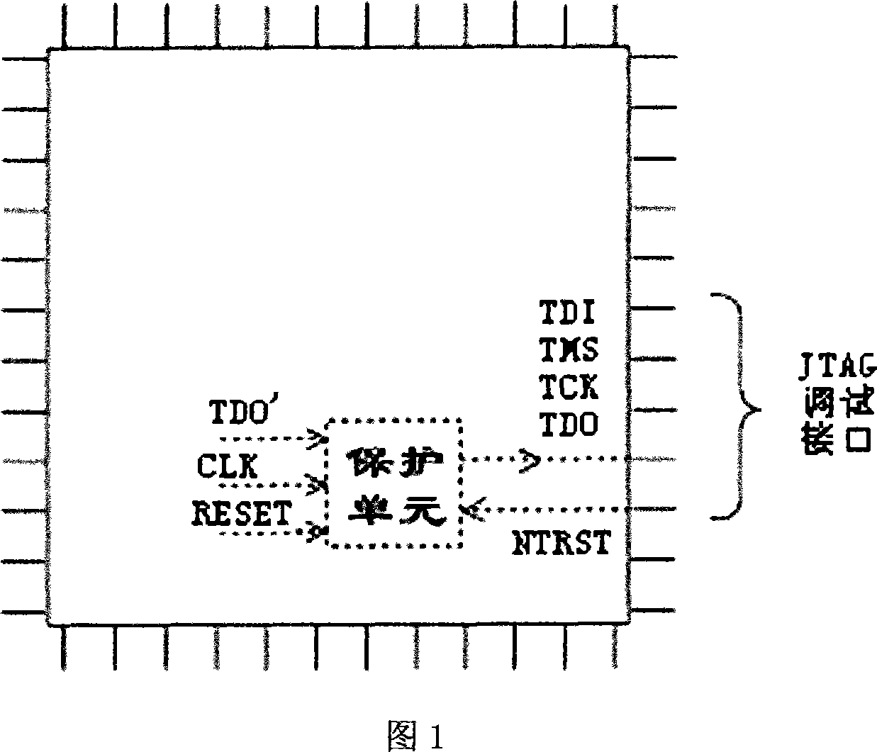
[0014] The present invention will be further described in detail below by taking the JTAG interface as an example in conjunction with the accompanying drawings and specific implementation methods.

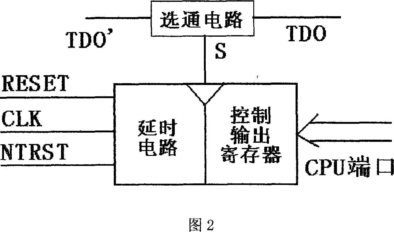
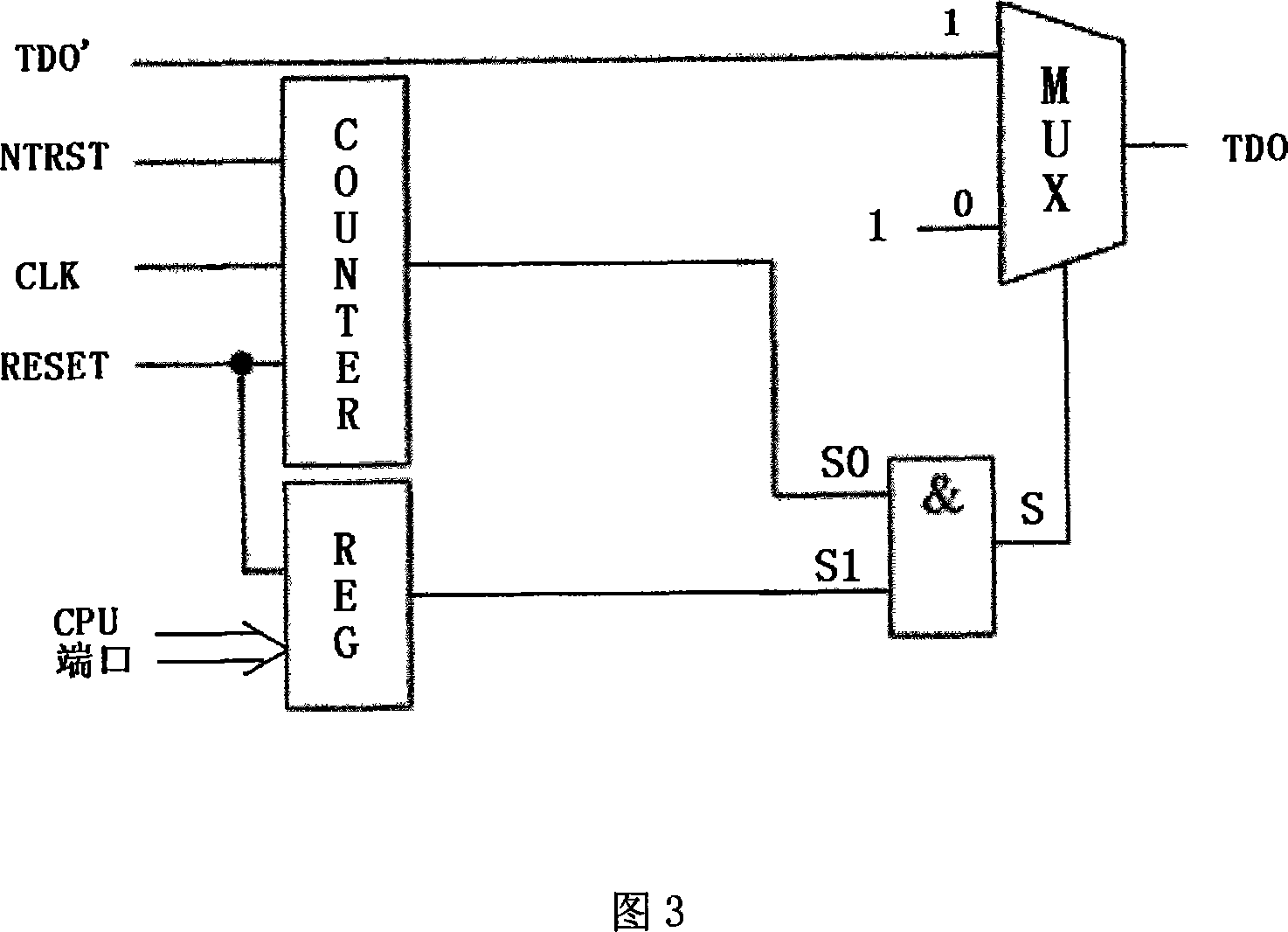
[0015] FIG. 2 is a circuit of the protection unit in FIG. 1 , and FIG. 3 is a specific embodiment of FIG. 2 .

[0016] The JTAG interface mainly has 5 signal lines, which are: test clock input TCK, test data input TDI, test data output TDO, test mode selection TMS, test reset TRST. Among them, TDO is the data output signal of the chip. As long as the signal is controlled, the internal information of the chip can be prevented from being read out. After the chip in the final product is started, the first instruction is to modify the control output register REG to invalidate the test data output TDO output of the JTAG interface, thereby achieving the purpose of protecting the chip code.

[0017] The specific implementation method is:

[0018] Find an empty address in the chip, desig...


PUM


Abstract

The invention provides a method for protecting chip data output signal and its circuit. The invention relates to an embedded chip interface, in particular to a method for protecting chip interface data output signal and its circuit. The data output signal in the chip is outputed by the pin line of chip output interface via the gating circuit. In the debug stage of system design, the time delay circuit in the control logic circuit, under the action of reset signal in the chip, generates the time delayed signal to act on the gating circuit for prohibiting data signal from being outputed and controlling the output controlling register in the logic circuit to output the default value, after signal is delayed, the gating circuit is allowed to output data signal. In the normal working stage of chip, the output controlling register in the control logic circuit recieves the read-in data instruction of CPU in the chip, in the effective date of time delayed signal, the read-in data instruction places the number for the output controlling register through the CPU port and prohibits the gating circuit from outputing data signal. The protection method and circuit has simple stucture, and can prevent the leakage of chip code without the special process.

Description

technical field [0001] The invention relates to an embedded chip interface, in particular to an interface data output signal protection method and a circuit thereof. Background technique [0002] Many embedded SOCs (System On Chip) are embedded with FLASH flash memory to reduce chip pins. The JTAG interface is a general debugging interface, which must be reserved for each SOC. Through the JTAG interface, data can be written to the embedded FLASH flash memory. , data can also be read out, so the code cannot be protected. The existing technology often adopts a fuse technology method. After the code is burned into the FLASH flash memory, the connection of the JTAG interface signal is fused inside the chip with the fuse technology. This method solves the problem of code protection from the source, but the fuse The silk process is a special process, which leads to problems such as increased chip costs and production difficulties. Contents of the invention [0003] The purpose...

Claims


Application Information

Patent Timeline
IPC IPC(8): G06F21/02G06F21/70
Inventor 刘新宁朱炜杨军王学香陆生礼时龙兴
Owner SOUTHEAST UNIV
Learn More