Mosfet power package

A power and die pad technology, applied in the direction of semiconductor/solid-state device parts, semiconductor devices, electrical components, etc., to save PCB space and optimize the layout of device leads

Inactive Publication Date: 2007-10-31
ALPHA & OMEGA SEMICON INC
View PDF0 Cites 1 Cited by
  • Summary
  • Abstract
  • Description
  • Claims
  • Application Information

AI Technical Summary

Problems solved by technology

[0003] Although the TO-252 package has two power MOSFETs in the common drain configuration shown in FIGS. Printed Circuit Board (PCB) use

Method used


Image

  • Mosfet power package
  • Mosfet power package
  • Mosfet power package

Examples


Embodiment Construction

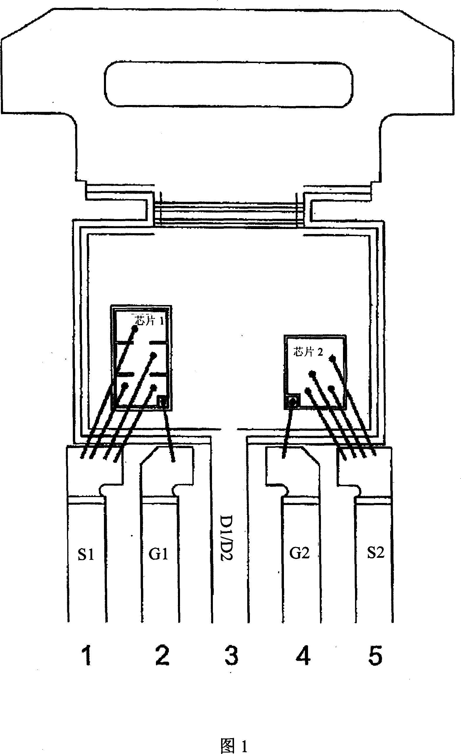
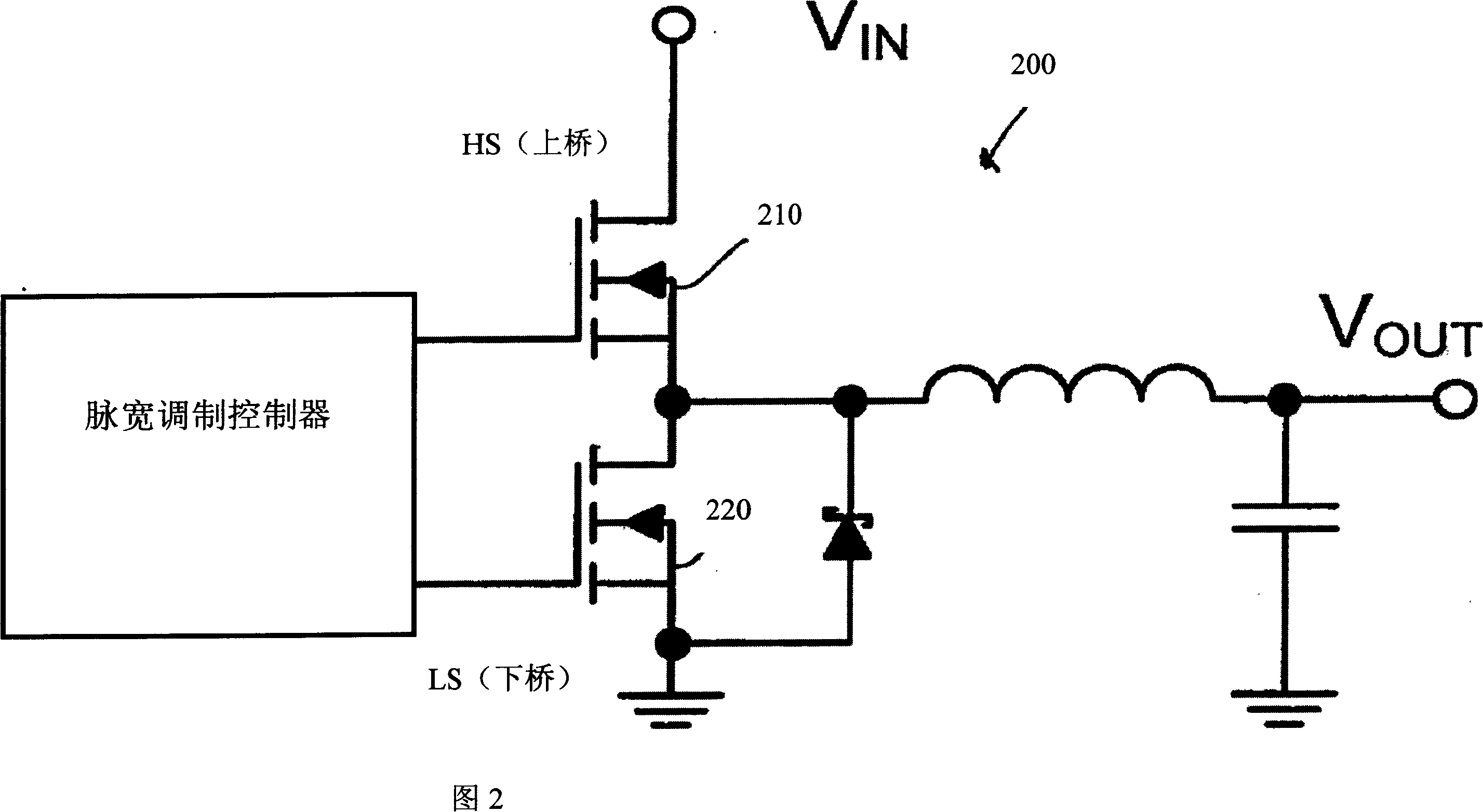
[0018] The invention provides a TO-252 power MOSFET package applied to a synchronous voltage converter. As shown in FIG. 5 , TO-252 package lead frame 500 includes a pair of drain pads 510 and 520 located above MOSFETs 515 and 525 respectively. After the connection portion 505 is trimmed along the dashed line A-A at the end of the packaging process, the drain pads 510 and 520 are insulated from each other, and the MOSFETs 515 and 525 are preferably soldered to the drain pads 510 and 520, respectively, or are bonded to the drain pads 510 and 520, respectively, using epoxy. Drain pads 510 and 520 are connected.

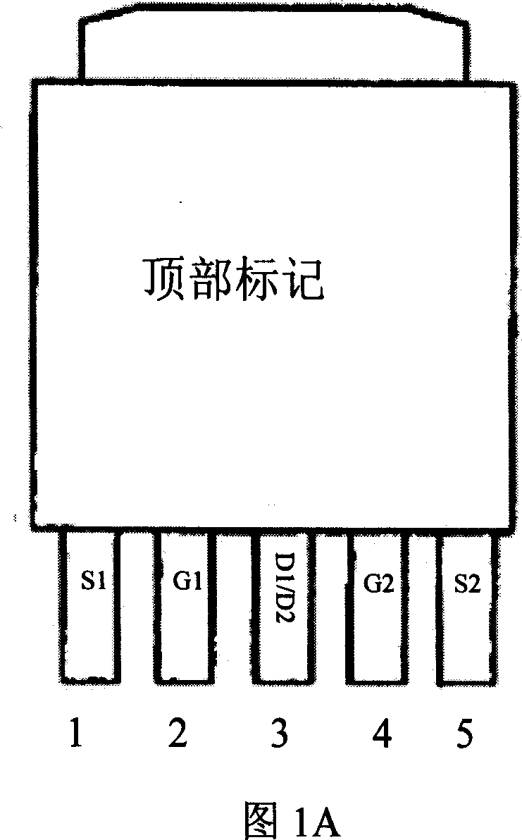
[0019] Wire bonder 530 connects the source of MOSFET 515 to drain pad 520, the gate of MOSFET 515 is wire bonded to gate lead G1 by wire bonder 517, and the source of MOSFET 525 is wire bonded to source lead by wire bonder 540 On S2 , the lead D1 is connected to the drain pad 510 , and the lead D2 / S1 is connected to the drain pad 520 .

[0020] FIG. 5A shows a TO-25...


PUM


Abstract

A power MOSFET package is disclosed. The power MOSFET package includes a leadframe having first and second die pads insulated one from the other, the first die pad being coupled to a first drain lead and the second die pad being coupled to a second drain lead. A first MOSFET device has a drain contact coupled-to the first die pad, a gate contact coupled to a first gate lead, and a source contact coupled to the second die pad. A second MOSFET device has a drain contact coupled to the second die pad, a gate contact coupled to a second gate lead, and a source contact coupled to a source lead. An encapsulant substantially encapsulates the leadframe, the first and second MOSFET devices and portions of the first and second gate leads, the first and second drain leads, and the source lead.

Description

technical field [0001] The present invention generally relates to a MOSFET power package. More specifically, the present invention relates to a 5-lead TO-252 power MOSFET package for a synchronous buck converter. Background technique [0002] Synchronous voltage converters provide high performance in a small footprint in portable battery-operated applications, including notebook computers. FIG. 2 shows a conventional synchronous voltage converter, indicated generally at 200 . A first N-channel enhancement MOSFET 210 and a second N-channel enhancement MOSFET 220 are connected together in a conventional manner, wherein the source of the first MOSFET 210 is connected to the drain of the second MOSFET 220 . [0003] Although the TO-252 package has two power MOSFETs in the common drain configuration shown in FIGS. printed circuit board (PCB) use. As shown in FIG. 3 , a high-side MOSFET 300 and a low-side MOSFET 310 are surface mounted on a PCB and connected to other component...

Claims


Application Information

Patent Timeline
Patent Type & Authority Applications(China)
IPC IPC(8): H01L25/00H01L25/07H01L23/488H01L23/495
CPCH01L2924/01015H01L23/49575H01L2224/0603H01L2924/01082H01L2924/00014H01L2224/06051H01L24/06H01L2224/85399H01L24/48H01L2924/01002H01L2224/48247H01L2224/45099H01L2924/13091H01L2924/01033H01L2924/19042H01L2924/01006H01L23/49562H01L2224/05552H01L2224/05599H01L2224/49111H01L2224/49171H01L2924/014H01L24/49H01L2924/00H01L2924/00012
Inventor 李文清骆建仁龚德梅
Owner ALPHA & OMEGA SEMICON INC
Why Eureka
Try Eureka