Magnetic memory device

A magnetic storage and magnetic field technology, applied in the field of writing magnetic storage devices and magnetic random access memory

Inactive Publication Date: 2007-11-07
HITACHI LTD +2
View PDF0 Cites 14 Cited by
  • Summary
  • Abstract
  • Description
  • Claims
  • Application Information

AI Technical Summary

Problems solved by technology

However, the write current required for the nanosecond period can be many times greater than the DC threshold current

Method used


Image

  • Magnetic memory device
  • Magnetic memory device
  • Magnetic memory device

Examples


no. 1 example

[0094] device design

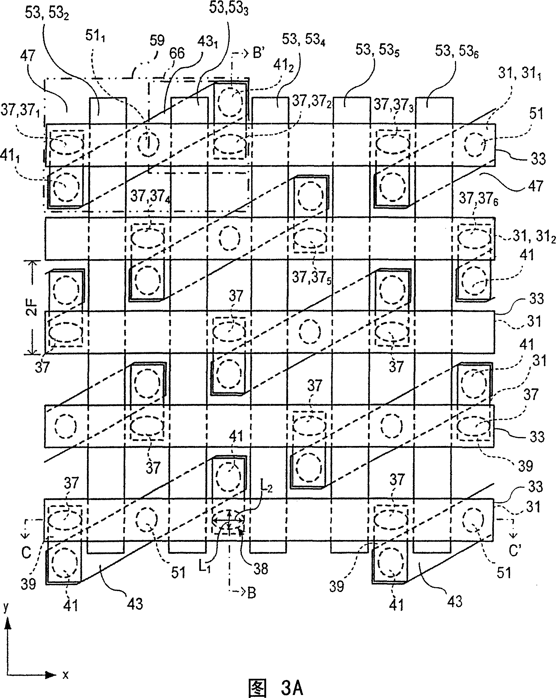
[0095] Referring to Figures 3A to 3D, a first embodiment of a memory array according to the present invention is shown. The memory array is Magnetic Random Access Memory (MRAM).

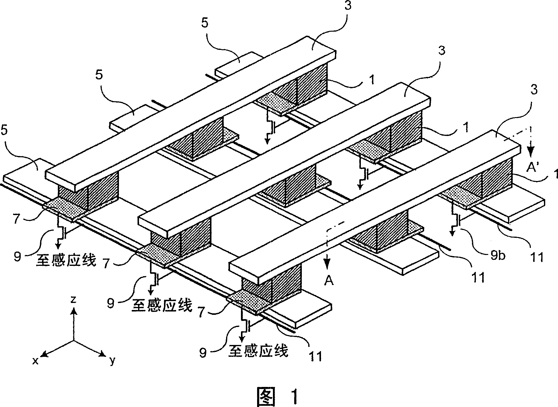
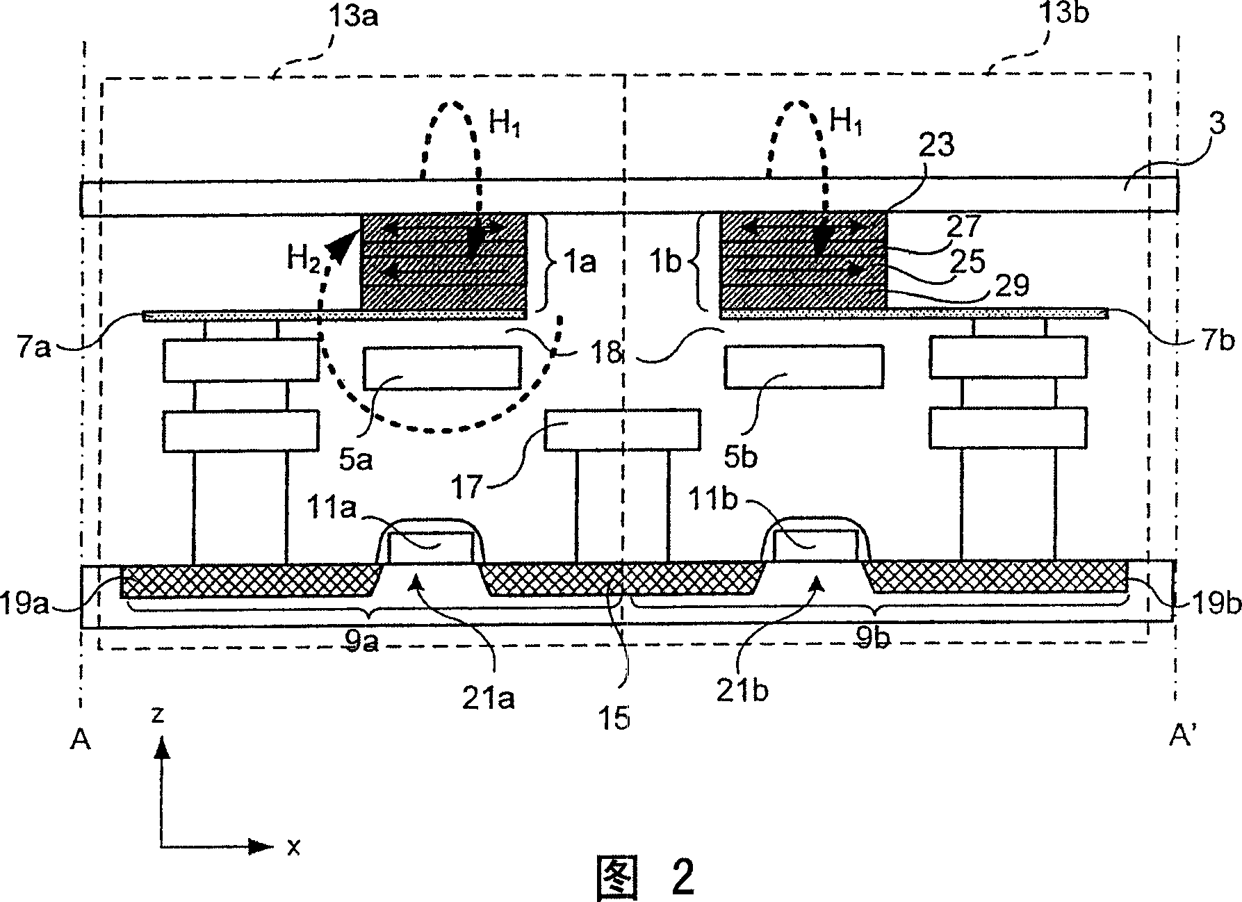
[0096] Specifically with reference to Fig. 3 A, memory array is made of a plurality of word lines 53 and a plurality of bit lines 31, and word line 53 has defined the first dimension of array, is the column of array in this example, and bit line 31 is positioned at word line 53 And perpendicular to the word lines 53, which define the second dimension of the array, in this case the rows of the array. A plurality of magnetic tunnel junctions (MTJs) 37 having stacked layers are connected to the lower side of each bit line 31 in the space between the word lines 53 .

[0097] The bit lines 31 are arranged in a first direction, defined here as the x-axis. The word lines 53 are arranged in a second direction, defined here as a y-axis.

[0098] Referring specifically to FIGS. 3B an...

no. 2 example

[0206] device design

[0207] Referring to Figures 12A to 12C, a second embodiment of a memory array according to the present invention is shown. The memory array is MRAM.

[0208]Referring specifically to FIG. 12A, a plurality of bit lines 201 are arranged in a first direction, here defined as the x-axis. Bit lines 201 define the first dimension of the array, in this example the rows of the array. The auxiliary current line 203 is located above each bit line 201 and is electrically insulated from the corresponding bit line 201 by an insulating matrix 205 .

[0209] Multiple MTJ207s are set. The MTJ 207 has the same structure as the MTJ 37 described above with reference to the first embodiment. Make the easy magnetization axis of MTJ 207 parallel to the bit line 201 , that is, parallel to the x-axis.

[0210] Referring specifically to FIG. 12B , each MTJ 207 is connected to the lower side of the bit line 201 . Therefore, MTJ 207 is electrically insulated from auxiliary c...


PUM

PropertyMeasurementUnit
Thicknessaaaaaaaaaa
Thicknessaaaaaaaaaa
Thicknessaaaaaaaaaa

Abstract

A magnetic memory device comprises a magnetic tunnel junction (MTJ) (37) connecting to a bit line (31) to a sense line (49) through an isolation transistor (81). The MTJ (37) includes a ferromagnetic layer having a magnetic hard axis. An assist current line (33) overlies the bit line (31) and is insulated from the bit line (31). The MTJ (37) is switchable between a first, relatively high resistance state and a second, relatively low resistance state. The assist current line (33) applies a magnetic field along the magnetic hard axis in the ferromagnetic layer, independently of current flow through the MTJ (37) for assisting switching of the MTJ (37) between the first and second states.

Description

technical field [0001] The present invention relates to a magnetic storage device, more specifically but not exclusively to a magnetic random access memory. The invention also relates to a method of writing to a magnetic memory device. Background technique [0002] The advent of Magnetic Random Access Memory (MRAM) is a promising step in the development of long-term as well as short-term data storage. MRAM has the benefit of non-volatility, and has lower power consumption and faster read and write times than flash memory (Flash) memory. MRAM also has lower power consumption than general-purpose volatile memories dynamic RAM (DRAM) and static RAM (SRAM), and faster read and write times than DRAM. [0003] A conventional MRAM cell includes a magnetic element having a ferromagnetic free layer and a ferromagnetic pinned layer separated by a nonmagnetic layer. The pinned layer has a relatively high coercivity such that its magnetisation remains fixed when a write magnetic fiel...

Claims


Application Information

Patent Timeline
IPC IPC(8): H01L43/08H01L27/22G11C11/16
CPCG11C11/16G11C11/1657G11C11/161G11C11/1659
Inventor 伊藤显知高桥宏昌河原尊之竹村理一郎蒂博·德沃尔代保罗·克罗扎约-冯·基姆克洛德·沙佩尔
Owner HITACHI LTD
Why Eureka
Try Eureka