

Liquid crystal display device and its driving method
A technology of a liquid crystal display and a driving method, applied in the field of liquid crystal displays and their driving, can solve the problems of picture distortion, pixel unit charging completion, waveform distortion, etc., and achieve the effect of avoiding data confusion
- Summary
- Abstract
- Description
- Claims
- Application Information
AI Technical Summary
Problems solved by technology
Method used
Image

Examples
Embodiment 1
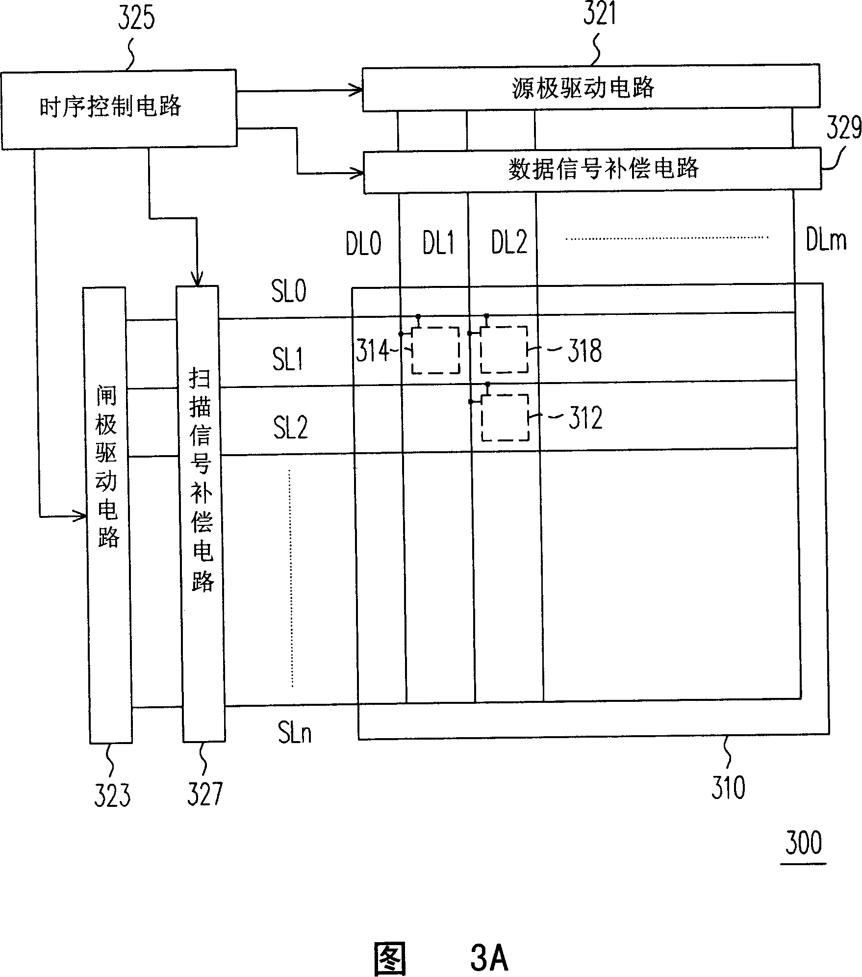
[0037] Please continue to refer to FIG. 3A . In order for those familiar with this technology to understand the spirit of the present invention, in the following embodiments, it is assumed that the specification of the liquid crystal display 300 is the 17 o'clock SXGA specification of the Video Electronics Standards Association (VESA) standard, but it does not The present invention is not limited thereto. According to the specification of SXGA at 17:00, the liquid crystal display 300 may have 1024 scan lines. The time spent by the gate driving circuit 323 in scanning the 1024 scan lines is referred to as the actual scan time hereinafter. After the gate drive circuit 323 scans the 1024 scan lines, the timing control circuit 325 controls the source drive circuit 321 and the gate drive circuit 323 to idle for a period of time, which is hereinafter referred to as blank scan time. The length of the blank scan time may be equivalent to the time it takes for the gate drive circuit ...
Embodiment 2
[0043] In Embodiment 2, the timing control circuit 325 controls the scan signal compensation circuit 327 to adjust the time length of the scan signal within the original actual scan time. Since the overall actual scan time remains unchanged, when the pixel units on the scan line closer to the source driving circuit 321 are enabled, the scan signal in this embodiment is shorter than the conventional scan signal. For example, when the pixel unit on the first scan line (SL0) is enabled, the scan signal can be adjusted to 14 microseconds, and when the pixel unit on the second scan line (SL1) is enabled, the scan signal can be increased is 14.2 microseconds, when the pixel unit on the third scanning line (SL2) is enabled, the scanning signal can be increased to 14.2 microseconds, and so on.
[0044] Similarly, the timing control circuit 325 controls the data signal compensation circuit 329 to adjust the time length of the data signal according to the adjusted time length of the sca...
Embodiment 3
[0047] In this embodiment, the methods of Embodiment 1 and 2 are combined. Specifically, the blank scan time is used to extend the actual scan time, and the timing control circuit 325 also controls the scan signal compensation circuit 327 to change the time length of the scan signal according to the position of the enabled pixel unit. In addition, the timing control circuit 325 also controls the data signal compensation circuit 329 to adjust the time length of the data signal according to the adjusted time length of the scan signal.
[0048] The advantage of this embodiment is that the time length of the data signal used to drive the pixel unit on the scan line (such as SL1024) far away from the source driver circuit can be increased considerably, so the data signal can have enough time to configure The pixel units on it are charged, so that the liquid crystal display 300 in this embodiment has better picture quality.
PUM
 Abstract
Description
Claims
Application Information