Liquid crystal display apparatus and method of restoring defected pixel

A liquid crystal display device, pixel electrode technology, applied in static indicators, nonlinear optics, instruments, etc., can solve problems such as defects, short-circuit bright spots or lines of pixel electrodes, etc. Effect

Inactive Publication Date: 2007-11-21
MITSUBISHI ELECTRIC CORP
View PDF1 Cites 3 Cited by
  • Summary
  • Abstract
  • Description
  • Claims
  • Application Information

AI Technical Summary

Problems solved by technology

Therefore, there is a possibility that the rolling of the conductive metal or the floating of the conductive metal lump may short-circuit between the pixel electrode and the counter electrode, thereby causing bright spots or line defects.

Method used


Image

  • Liquid crystal display apparatus and method of restoring defected pixel
  • Liquid crystal display apparatus and method of restoring defected pixel
  • Liquid crystal display apparatus and method of restoring defected pixel

Examples


Embodiment approach 1

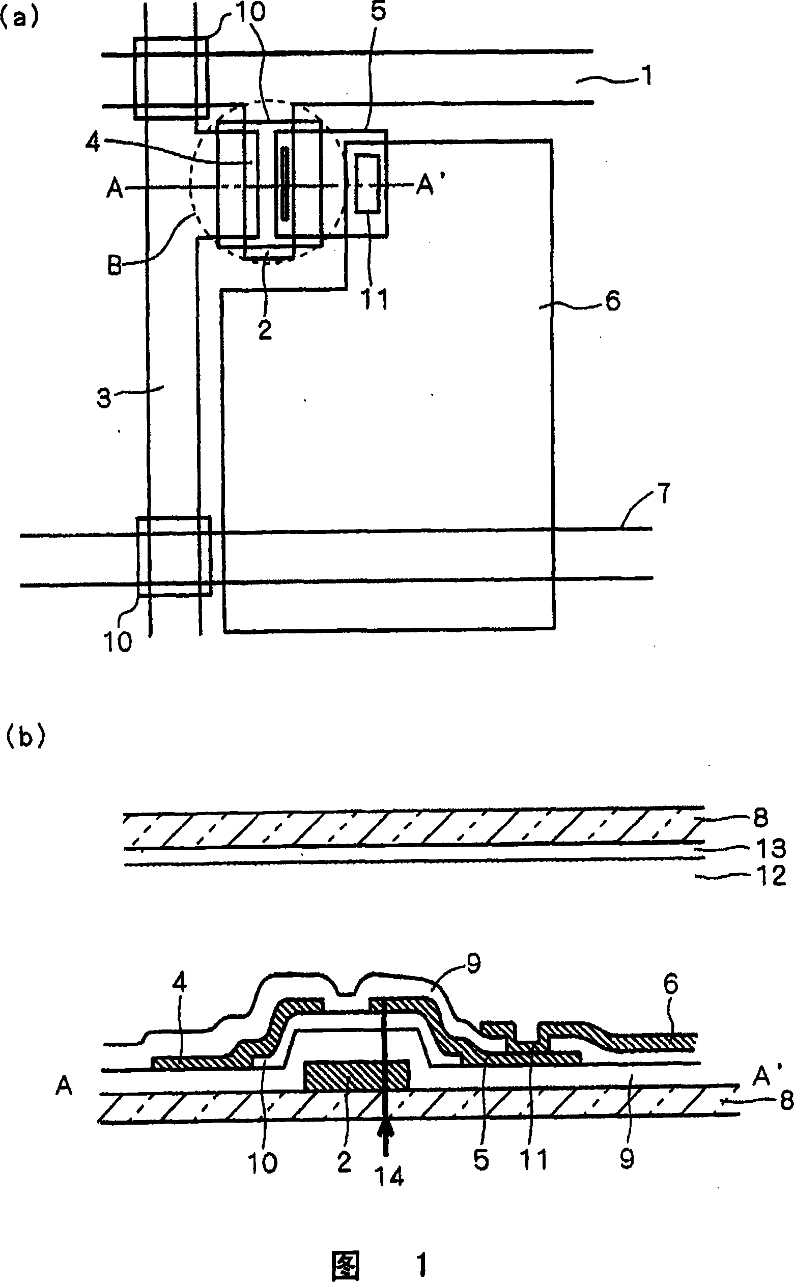
[0022] 1( a ), ( b ) show a plan view and a cross-sectional view of a liquid crystal display device according to this embodiment. Wherein, Fig. 1(a) shows a plan view of a pixel portion of the array substrate, and Fig. 1(b) shows a cross-sectional view along A-A' of Fig. 1(a). The liquid crystal display device of this embodiment has a structure in which pixels are arranged in a matrix, and each pixel is driven by a thin film transistor (TFT) which is a thin film active element.

[0023] In the liquid crystal display device of this embodiment, as shown in FIGS. An insulating film 9 is provided in two layers, and an amorphous silicon (a-Si) film 10 as a semiconductor active film is provided in a third layer. Furthermore, in the liquid crystal display device of this embodiment, the source wiring 3, the source electrode 4, and the drain electrode 5 are provided in the fourth layer, the insulating film 9 is provided in the fifth layer, and finally the pixel electrode 6 is provided...

Embodiment approach 2

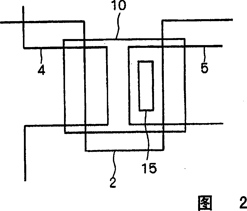
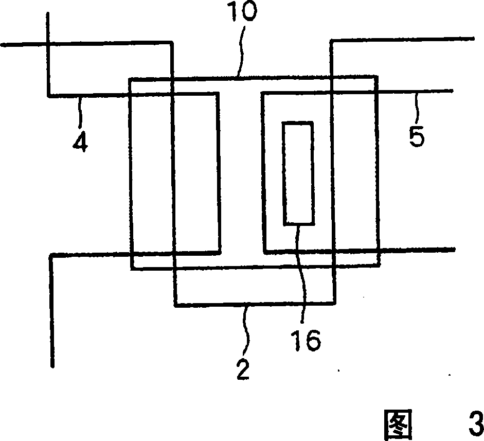
[0034] FIG. 3 is an enlarged view showing a TFT of the liquid crystal display device of the present embodiment. In FIG. 3 , a hole 16 is provided on the drain electrode 5 at a position where the gate electrode 2 and the drain electrode 5 planarly overlap each other. The hole 16 provided may have any shape as long as it is located at a position where the gate electrode 2 and the drain electrode 5 planarly overlap each other. In addition, in the present embodiment, the hole 15 is not provided on the gate electrode 2 .

[0035] In addition, in this embodiment, since the hole 15 is not opened in the gate electrode 2, the position of the hole 16 provided in the drain electrode 5 cannot be confirmed from the glass substrate side. Therefore, when a bright spot defect caused by a malfunction of the TFT occurs, as shown in FIG. The hole 16 is used to determine the irradiation position of the laser light 14 .

[0036] However, compared with the case where the gate electrode 2 and the...

Embodiment approach 3

[0039] The structure of the liquid crystal display device of Embodiment 1 is such that, as shown in FIG. 2 , a hole 15 is provided in the gate electrode 2 at a position where the gate electrode 2 and the drain electrode 5 planarly overlap each other. On the other hand, the structure of the liquid crystal display device according to the second embodiment is such that, as shown in FIG. 3 , hole 16 is provided in drain electrode 5 at a position where gate electrode 2 and drain electrode 5 planarly overlap each other.

[0040] The liquid crystal display device of this embodiment employs a combination of Embodiment 1 and Embodiment 2. That is, the structure of the liquid crystal display device of the present embodiment is: the hole 15 is provided on the gate electrode 2 at the position where the gate electrode 2 and the drain electrode 5 planarly overlap each other, and the hole 15 is provided at the position where the gate electrode 2 and the drain electrode 5 planarly overlap each...


PUM


Abstract

The invention provides a liquid crystal display device which has clear irradiation positions of laser beams, has a shape of gate electrode or drain electrode assuring the reliable repair and can suppress rolling-up of conductive metal or scattering of metal lump, and to provide a method of restoring defective pixel of the liquid crystal display device. The liquid crystal display device comprises: a plurality of gate lines 1; a plurality of source lines 3 formed so as to substantially orthogonal to the gate lines 1; pixel electrodes 6 formed in a matrix shape every intersection parts between the gate lines 1 and the source lines 3; gate electrodes 2 connected to the gate lines 1; source electrodes 4 connected to the source lines 3; drain electrodes 5 connected to the pixel electrodes 6; and TFTs formed correspondingly to respective pixel electrodes 6. Therein, the TFTs are provided with holes 15, 16 on at least one of the gate electrodes 2 and the drain electrodes 5 on the position where the gate electrodes 2 and the drain electrodes 5 are planarly superimposed on each other.

Description

technical field [0001] The present invention relates to a liquid crystal display device and a method for repairing defective pixels thereof, in particular to a liquid crystal display device and a method for repairing defective pixels thereof capable of repairing defective pixels caused by a malfunction of a thin film active element. Background technique [0002] A general method of manufacturing a liquid crystal display device including a thin film transistor (hereinafter also referred to as TFT) is as follows. First, a gate wiring and a gate electrode are formed on a glass substrate (transparent insulating substrate), and an insulating film is formed thereon. Furthermore, an amorphous silicon (a-Si) film as a semiconductor active film is formed on the insulating film. Then, a source wiring, a source electrode, and a drain electrode are formed on the amorphous silicon film, an insulating film is laminated thereon, and finally a pixel electrode is forme...

Claims


Application Information

Patent Timeline
Patent Type & Authority Applications(China)
IPC IPC(8): G02F1/1362G02F1/13G09G3/36
CPCG02F1/136259G02F1/1368G02F2001/136268G02F1/136268G02F1/136G02F1/1343
Inventor 山下真司
Owner MITSUBISHI ELECTRIC CORP
Why Eureka
Try Eureka