Nitride-based semiconductor light emitting diode

A nitride semiconductor, nitride-based technology, applied in semiconductor devices, electrical components, circuits, etc., can solve the problems of reducing the reliability and yield of nitride-based semiconductor LEDs, and unstable characteristics of nitride-based semiconductor LEDs.

Inactive Publication Date: 2007-11-21
SAMSUNG ELECTRO MECHANICS CO LTD
View PDF1 Cites 12 Cited by
  • Summary
  • Abstract
  • Description
  • Claims
  • Application Information

AI Technical Summary

Problems solved by technology

[0016] Therefore, such a structure is a major cause of instability in the characteristics of nitride-based semiconductor LEDs, thereby reducing the reliability and yield of nitride-based semiconductor LEDs.

Method used


Image

  • Nitride-based semiconductor light emitting diode
  • Nitride-based semiconductor light emitting diode
  • Nitride-based semiconductor light emitting diode

Examples


no. 1 example

[0039] First, a nitride-based semiconductor LED according to a first embodiment of the present invention will be described with reference to FIGS. 4 and 5 .

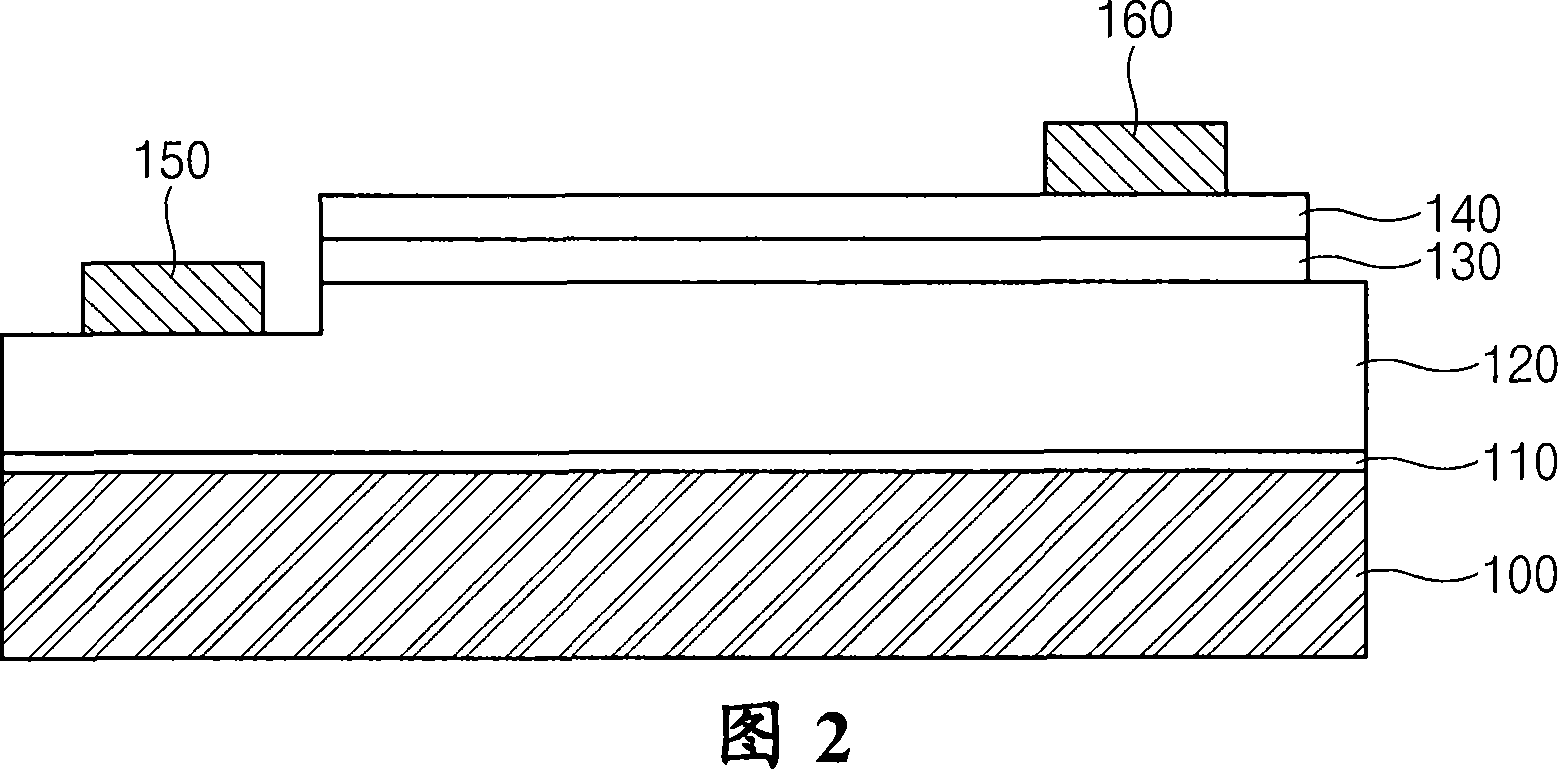
[0040] 4 is a plan view showing the structure of a nitride-based semiconductor LED according to a first embodiment of the present invention, and FIG. 5 is a cross-sectional view taken along line V-V' of FIG. 4 .

[0041] As shown in FIG. 4 and FIG. 5, the nitride-based semiconductor LED according to the first embodiment of the present invention includes an optically transparent substrate 100 and a light emitting structure, wherein a buffer layer 110, an n-type nitride semiconductor layer 120, an active layer 130 , and a p-type nitride semiconductor layer 140 are sequentially laminated on the substrate 100 .

[0042] The substrate 100 may be a heterogeneous substrate, such as a sapphire substrate and a silicon carbide (SiC) substrate, or a homogeneous substrate, such as a nitride substrate, which is suitable for growing a...

no. 2 example

[0059] Next, a nitride-based semiconductor LED according to a second embodiment of the present invention will be described in detail with reference to FIG. 7 . However, descriptions of components in the second embodiment that are the same as those in the first embodiment will be omitted.

[0060] Fig. 7 is a plan view showing the structure of a nitride-based semiconductor LED according to a second embodiment.

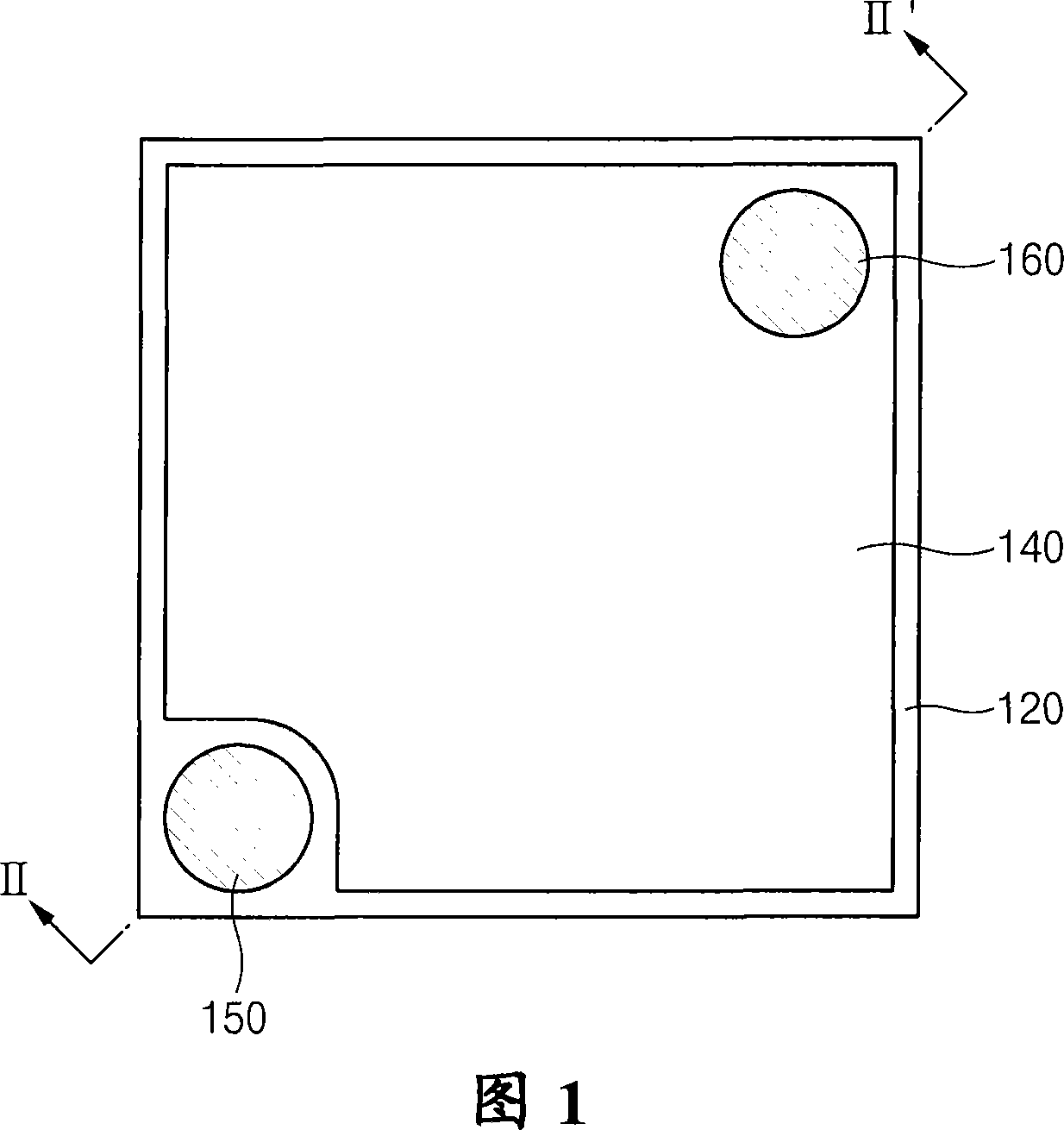
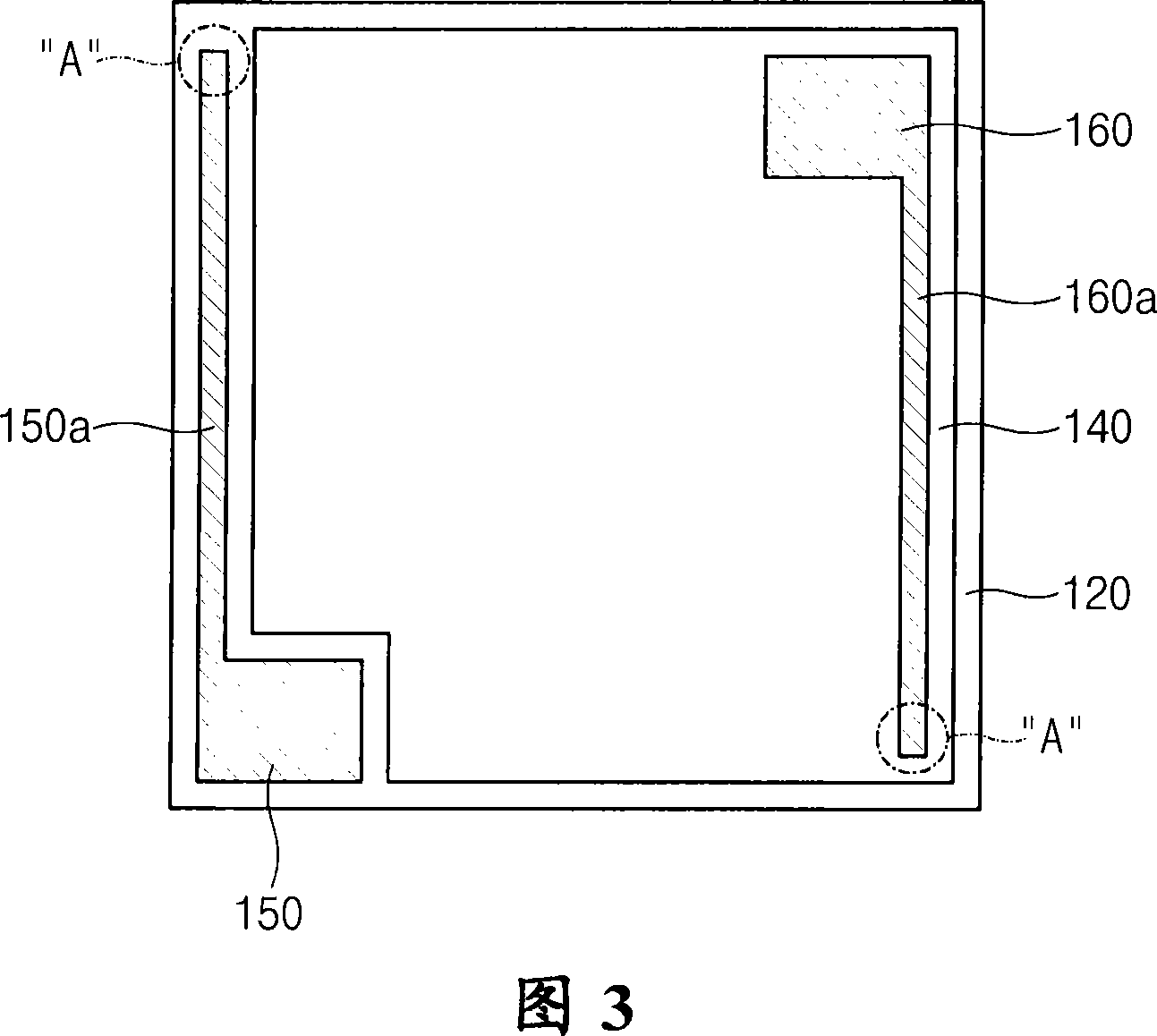
[0061] As shown in FIG. 7, the nitride-based semiconductor LED according to the second embodiment has almost the same structure as that of the nitride-based semiconductor LED according to the first embodiment. However, in the second embodiment, the n-electrode 150 and the p-electrode 160 are formed in a hemispherical shape instead of a rectangular shape. In addition, two p-type branch electrodes 160a are arranged in a finger shape so that the p-type branch electrodes 160a are parallel to each other.

[0062] Similar to the first embodiment, n-type and p-type ESD pads ...


PUM


Abstract

A nitride-based semiconductor LED comprises a substrate; an n-type nitride semiconductor layer formed on the substrate; an active layer formed on a predetermined region of the n-type nitride semiconductor layer; a p-type nitride semiconductor layer formed on the active layer; a p-electrode formed on the p-type nitride semiconductor layer, the p-electrode having a p-type branch electrode; a p-type ESD pad formed at the end of the p-type branch electrode, the p-type ESD pad having a larger width than the end of the p-type branch electrode; an n-electrode formed on the n-type nitride semiconductor layer, on which the active layer is not formed, the n-electrode having an n-type branch electrode; and an n-type ESD pad formed at the end of the n-type branch electrode, the n-type ESD pad having a larger width than the end of the n-type branch electrode.

Description

[0001] Related Application Cross Reference [0002] This application claims the benefit of Korean Patent Application No. 10-2006-0043986 filed with the Korean Intellectual Property Office on May 16, 2006, the disclosure of which is incorporated herein by reference. technical field [0003] The present invention relates to a nitride-based semiconductor light emitting diode in which a p-electrode and an n-electrode having high resistance to electrostatic discharge (hereinafter, referred to as ESD) have a lateral structure. Background technique [0004] In general, a light emitting diode (hereinafter, referred to as LED) is a semiconductor element that converts electrical signals into infrared rays, visible rays, or light rays using characteristics of compound semiconductors (ie, recombination of electrons and holes), for sending and receiving signals. [0005] LEDs are generally used in home appliances, remote controls, electronic signage, displays, various automation equipme...

Claims


Application Information

Patent Timeline
Patent Type & Authority Applications(China)
IPC IPC(8): H01L33/00H01L33/32H01L33/38H01L33/42
CPCH01L33/20H01L33/38
Inventor 高健维吴邦元黄硕珉金制远朴亨镇金东佑
Owner SAMSUNG ELECTRO MECHANICS CO LTD
Why Eureka
Try Eureka