Method for forming tantalum nitride film
A nitride film and compound technology, applied in gaseous chemical plating, coatings, electrical components, etc., can solve different problems and achieve the effect of high Ta/N composition ratio
- Summary
- Abstract
- Description
- Claims
- Application Information
AI Technical Summary
Problems solved by technology
Method used
Image
Examples
Embodiment 1
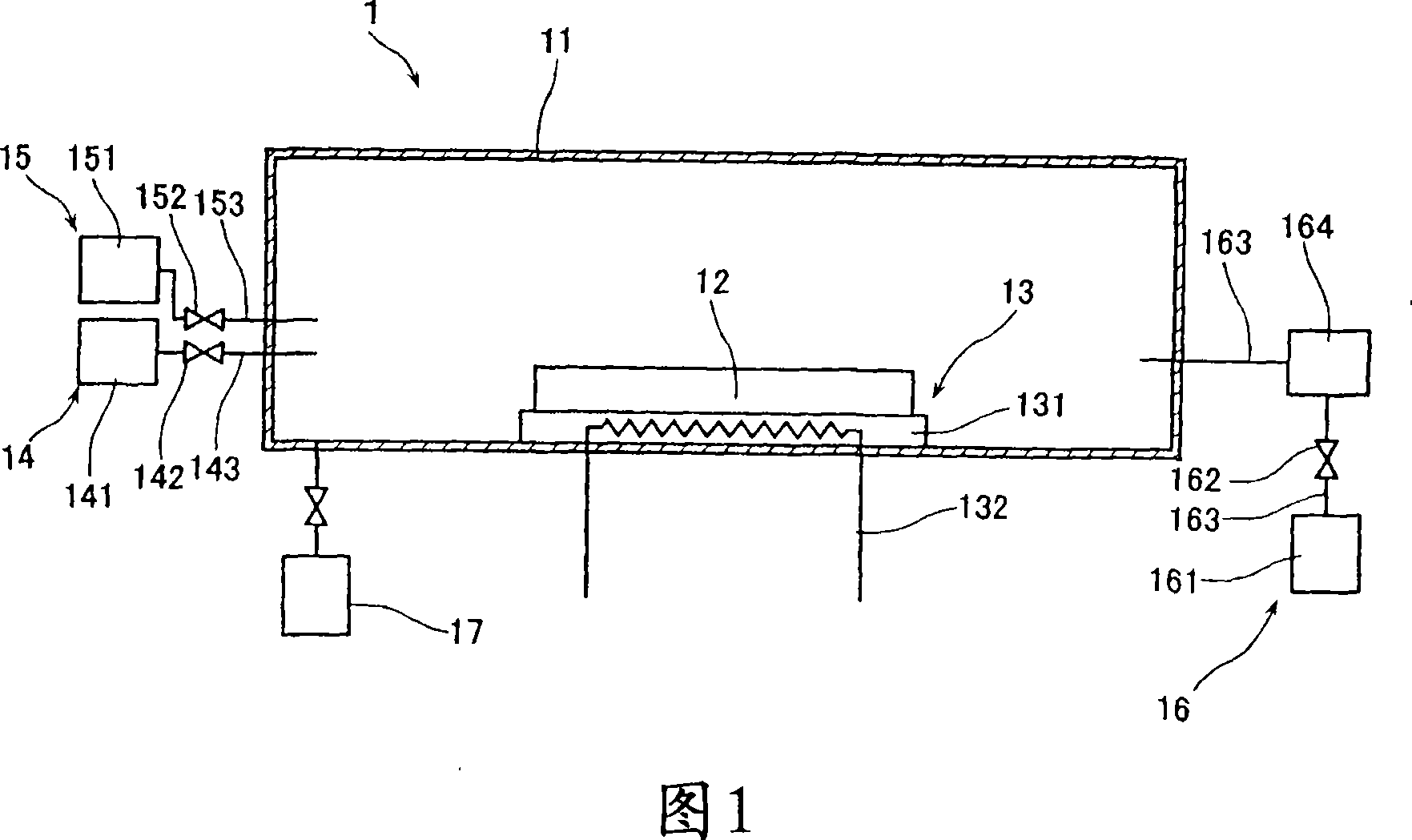
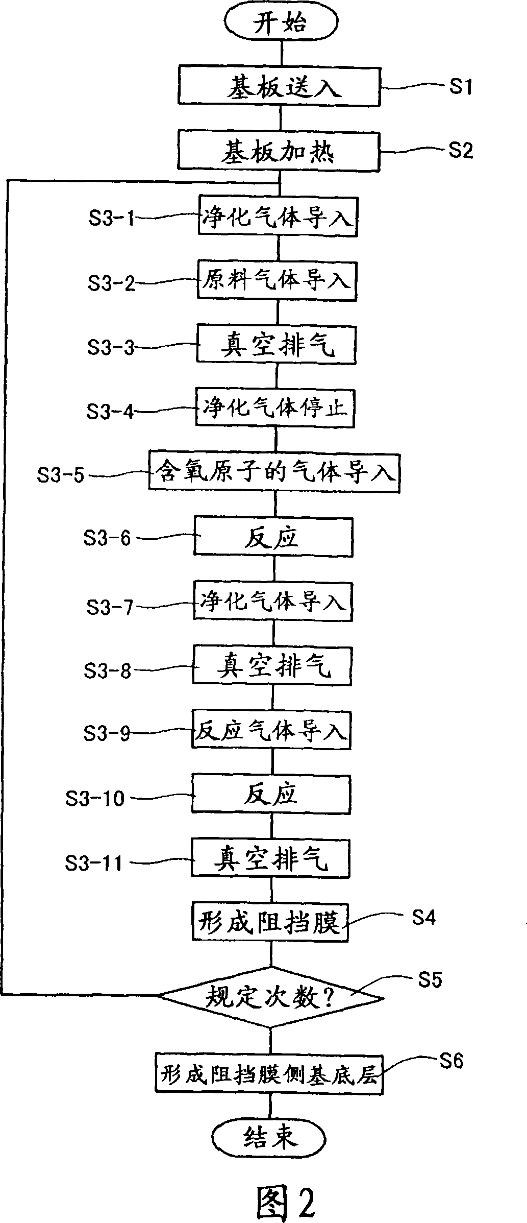
[0094] In this example, using the film forming apparatus 1 shown in FIG. 1, penta(dimethylamino)tantalum (MO) gas was used as a source gas, and O 2 gas, and as a reactive gas, use H 2 gas, according to the process flow chart shown in Figure 2 to form a tantalum nitride film.
[0095] According to known methods, in the implementation with SiO 2 After the degassing pretreatment process on the surface of the substrate 12 of the insulating film, utilize a vacuum exhaust system 17 to vacuum exhaust to 10 -5 In the film forming apparatus 1 below Pa, the substrate 12 is carried in (S1). The substrate is not particularly limited, and for example, a substrate in which a voltage is applied to a target having Ta as a main component using Ar sputtering gas according to a common sputtering method to generate plasma and sputter A target is a substrate on which an adhesive layer on the substrate side is formed on the surface.
[0096] After the substrate 12 is carried into the film formi...
Embodiment 2
[0113] In this example, using the film forming apparatus 1 shown in FIG. 2 gas, and the use of H as a reactive gas 2 gas, and form a tantalum nitride film according to the process flow chart shown in FIG. 5 .
[0114] Operated in the same manner as in Example 1, the substrate 12 that had carried out the surface degassing pretreatment process was sent into and utilized the vacuum exhaust system 17 to vacuum exhaust to 10 -5 In the film formation apparatus 1 below Pa (S1).
[0115] After carrying in the substrate 12, depending on the occasion, for example, Ar as a sputtering gas is introduced from the sputtering gas introduction system 20 (S2), a voltage is applied from the voltage application device 19 to the target 18 containing Ta to generate plasma (S3), For the sputtering target 18, a metal thin film, that is, a substrate-side adhesive layer may be formed on the surface of the substrate 12 (S4).
[0116] After the step S4 is completed, the substrate 12 is heated to 250° ...
Embodiment 3
[0127] As the raw material gas, instead of penta(dimethylamino)tantalum, tert-amyliminotris(dimethylamino)tantalum was used, and when the film formation process was carried out according to Example 1, Ta-rich low-resistance tantalum nitride film. For the obtained film, Ta / N=1.8, C content: 1%, N content: 35.7%, and the resistivity of the obtained thin film was 1000 μΩ·cm.
PUM
| Property | Measurement | Unit |
|---|---|---|
| electrical resistivity | aaaaa | aaaaa |
| electrical resistivity | aaaaa | aaaaa |
| electrical resistivity | aaaaa | aaaaa |
Abstract
Description
Claims
Application Information


