Method for manufacturing a periodically-poled structure

A manufacturing method and polarization technology, applied in the fields of nonlinear optics, instruments, optics, etc., can solve the problems such as the failure to improve the manufacturing yield of wavelength conversion elements, crystal damage, etc.

Inactive Publication Date: 2007-12-19
NIPPON TELEGRAPH & TELEPHONE CORP +1
View PDF0 Cites 4 Cited by
  • Summary
  • Abstract
  • Description
  • Claims
  • Application Information

AI Technical Summary

Problems solved by technology

As a result, in the single-domain secondary nonlinear optical crystal, the strong thermoelectric effect caused by the heating or cooling process of the electrode pattern manufacturing process will lead to the damage of the crystal itself.
For this reason, there is a problem that the manufacturing yield of the wavelength conversion element cannot be improved.

Method used


Image

  • Method for manufacturing a periodically-poled structure
  • Method for manufacturing a periodically-poled structure
  • Method for manufacturing a periodically-poled structure

Examples


Embodiment 1

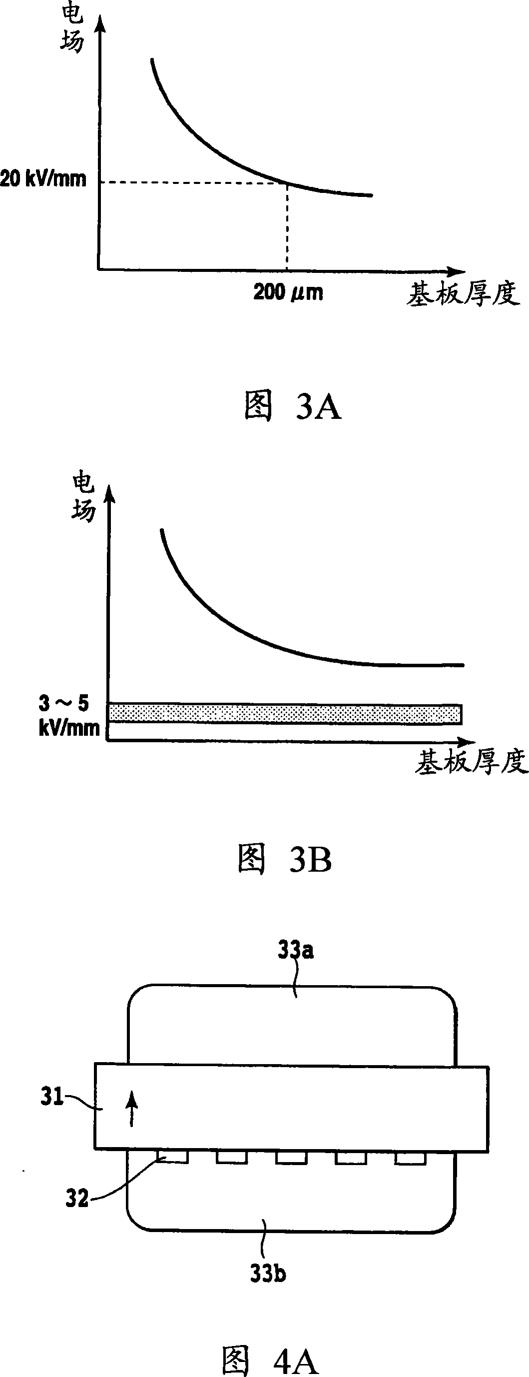
[0041] FIG. 5 shows a method of manufacturing the periodic polarization inversion structure according to the first embodiment. In Example 1, a 3-inch Zn-doped LN substrate with a substrate thickness of 300 μm was used as the secondary nonlinear optical crystal. The LN substrate 41 is mono-domained, and a resist pattern 42 corresponding to a periodic polarization inversion structure is formed on the -Z surface.

[0042] Fabrication of the resist pattern 42 is performed by an ordinary photolithography process. After the organic cleaning, the surface of the LN substrate 41 is subjected to lipophilic treatment, and then S1818 resist (Resist) manufactured by Shipley Co., Ltd. is dropped on the substrate to carry out spin coating. The resist film after spin coating is Drying and curing by baking in a constant temperature oven. The substrate will not be damaged by heating during coating or subsequent cooling. This is because the substrate thickness of the LN substrate 41 is 300 mi...

Embodiment 2

[0047] In Example 2, the same method as in Example 1 was used to fabricate a periodic polarization inversion structure on a 3-inch Zn-doped LN substrate with a substrate thickness of 5 mm. Manufacture of a resist pattern corresponding to a periodic polarization structure was carried out in the same manner as in Example 1, and a resist pattern with a period of 4.5 microns was produced.

[0048] FIG. 6 shows a method of manufacturing the periodic polarization inversion structure according to the second embodiment. In Example 2, the polarization inversion structure was produced in a state where the LN substrate 41 was heated by housing the container 43 used in Example 1 in a mantle heater. The container 43 is made of polycarbonate having excellent heat resistance. Here, the thermocouple 52 was heated to 90° C. in a state where the container 43 was housed. The LN substrate 41 is not damaged during heating. This is because the LN substrate 41 has a thickness of 5 mm and is highl...

Embodiment 3

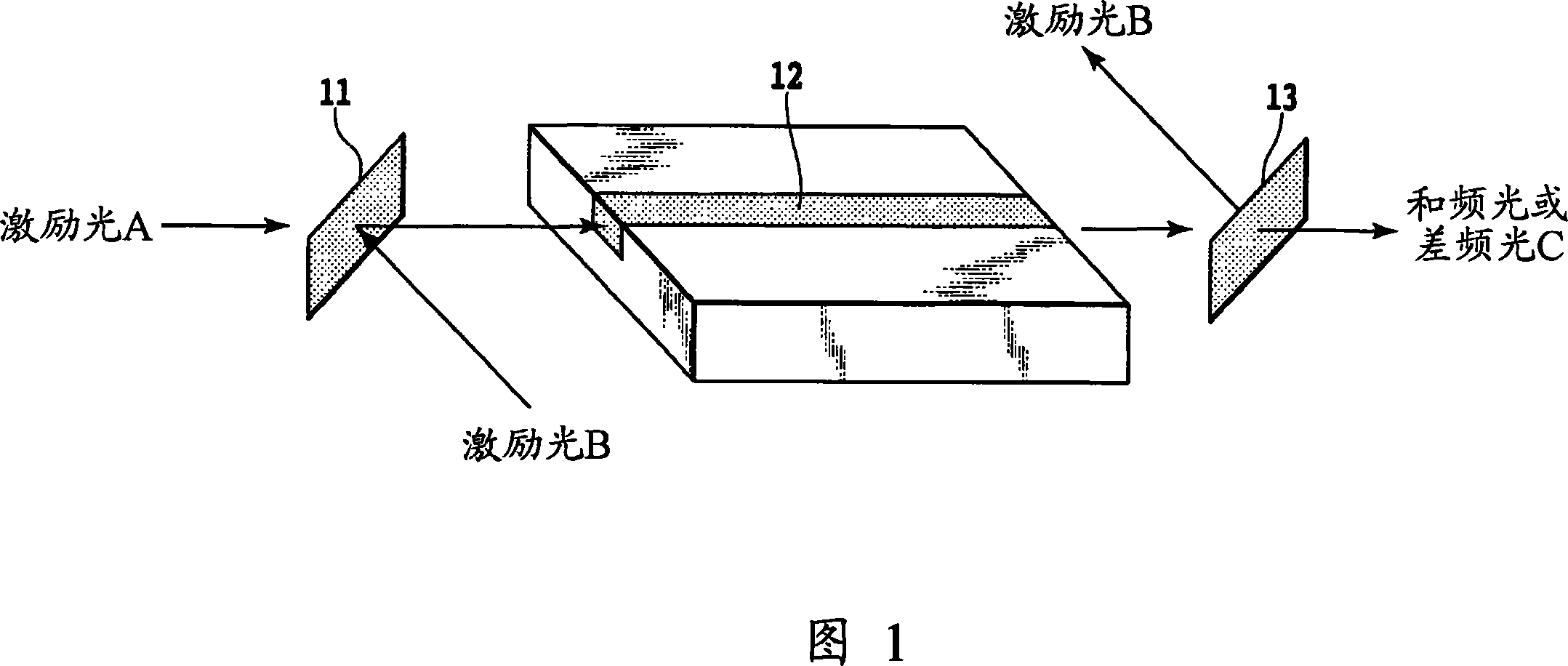
[0053] In the same manner as in Example 1, a periodic polarization inversion structure was fabricated using a 3-inch Zn-doped LN substrate with a substrate thickness of 300 μm. Manufacture of a resist pattern corresponding to a periodic polarization structure was carried out in the same manner as in Example 1, and a resist pattern with a period of 28.5 microns was produced. A strip-shaped element is cut out from the produced LN substrate in a direction perpendicular to the periodic polarization inversion structure, and then both end surfaces of the cut element are ground. When excitation light with a wavelength of 1560 nm and excitation light with a wavelength of 1060 nm are incident on the element in a direction perpendicular to the periodic polarization inversion structure, difference frequency light as mid-infrared light with a wavelength of 3.3 μm can be generated.


PUM

PropertyMeasurementUnit
thicknessaaaaaaaaaa
thicknessaaaaaaaaaa
thicknessaaaaaaaaaa

Abstract

There is provided a periodical polarization inversion structure manufacturing method having a high conversion efficiency and a high manufacturing yield. The method manufactures a periodical polarization inversion structure in a second-order nonlinear optical crystal (31) formed into a single domain. The method includes a step for forming a resist pattern (32) matched with the polarization inversion period on the -Z plane of the second-order nonlinear optical crystal (31), and a step for applying voltage so as to apply an electric field to the second-order nonlinear optical crystal (31) with the -Z plane having the resist pattern (32) as a negative voltage and the +Z plane as a positive voltage. The second-order nonlinear optical crystal (31) contains at least one element as an additive for compensating the defect of the crystal.

Description

technical field [0001] The present invention relates to a method for fabricating a periodic polarization inversion structure, and more particularly, to a method for fabricating a period polarization inversion structure in a quadratic nonlinear optical crystal for use in applications expected as visible light lasers. Or a quasi-phase-matched wavelength conversion element that is practical for mid-infrared lasers. Background technique [0002] Conventionally, as a wavelength converting element for converting the wavelength of light, an element using a semiconductor optical amplifier, an element using four-wave mixing, and the like are known. However, these conversion elements cannot meet the conditions of high efficiency, high speed, wide frequency, low noise and polarization insensitivity required by the system. [0003] On the one hand, it is expected that wavelength conversion elements utilizing second harmonics, sum frequencies, and difference frequencies generated by pse...

Claims


Application Information

Patent Timeline
Patent Type & Authority Applications(China)
IPC IPC(8): G02F1/37
CPCG02F1/3558
Inventor 铃木博之遊部雅生梅木毅伺西田好毅忠永修柳川勉曲克明马渡宏泰宫泽弘汤本润司
Owner NIPPON TELEGRAPH & TELEPHONE CORP
Why Eureka
Try Eureka