Epitaxial wafer manufacturing method and epitaxial wafer

A manufacturing method and epitaxial technology, applied in the fields of semiconductor/solid-state device manufacturing, electrical components, circuits, etc., can solve problems such as reduced productivity and increased cost, and achieve high productivity, improved productivity, and excellent film thickness uniformity.

Inactive Publication Date: 2007-12-19
SHIN-ETSU HANDOTAI CO LTD
View PDF1 Cites 5 Cited by
  • Summary
  • Abstract
  • Description
  • Claims
  • Application Information

AI Technical Summary

Problems solved by technology

But growing thicker epitaxial layers at low rates leads to even lower productivity and significantly higher costs

Method used


Image

  • Epitaxial wafer manufacturing method and epitaxial wafer
  • Epitaxial wafer manufacturing method and epitaxial wafer
  • Epitaxial wafer manufacturing method and epitaxial wafer

Examples


Embodiment

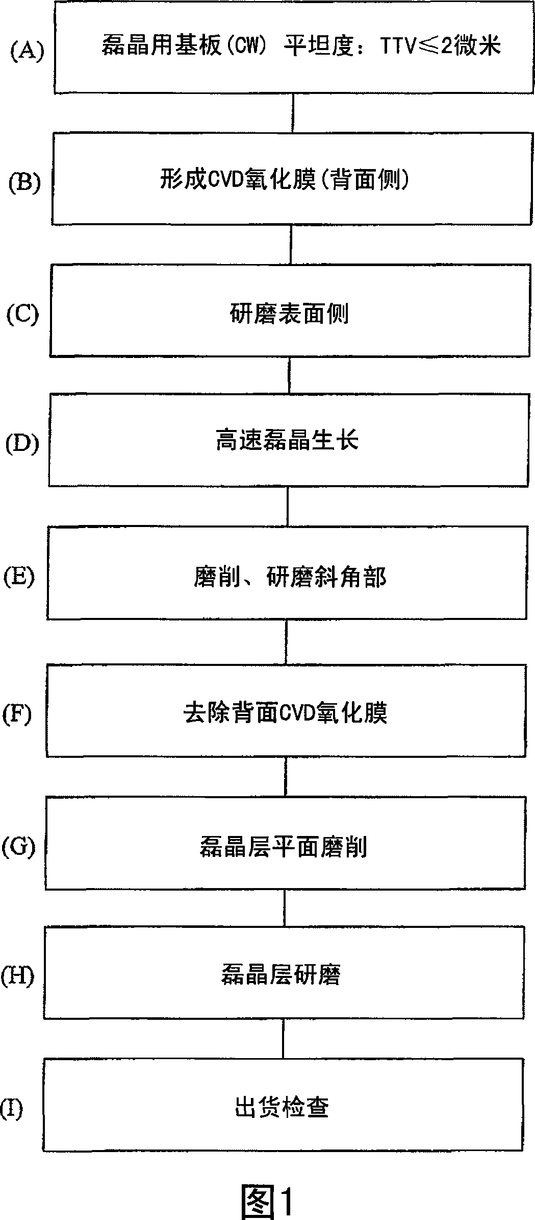
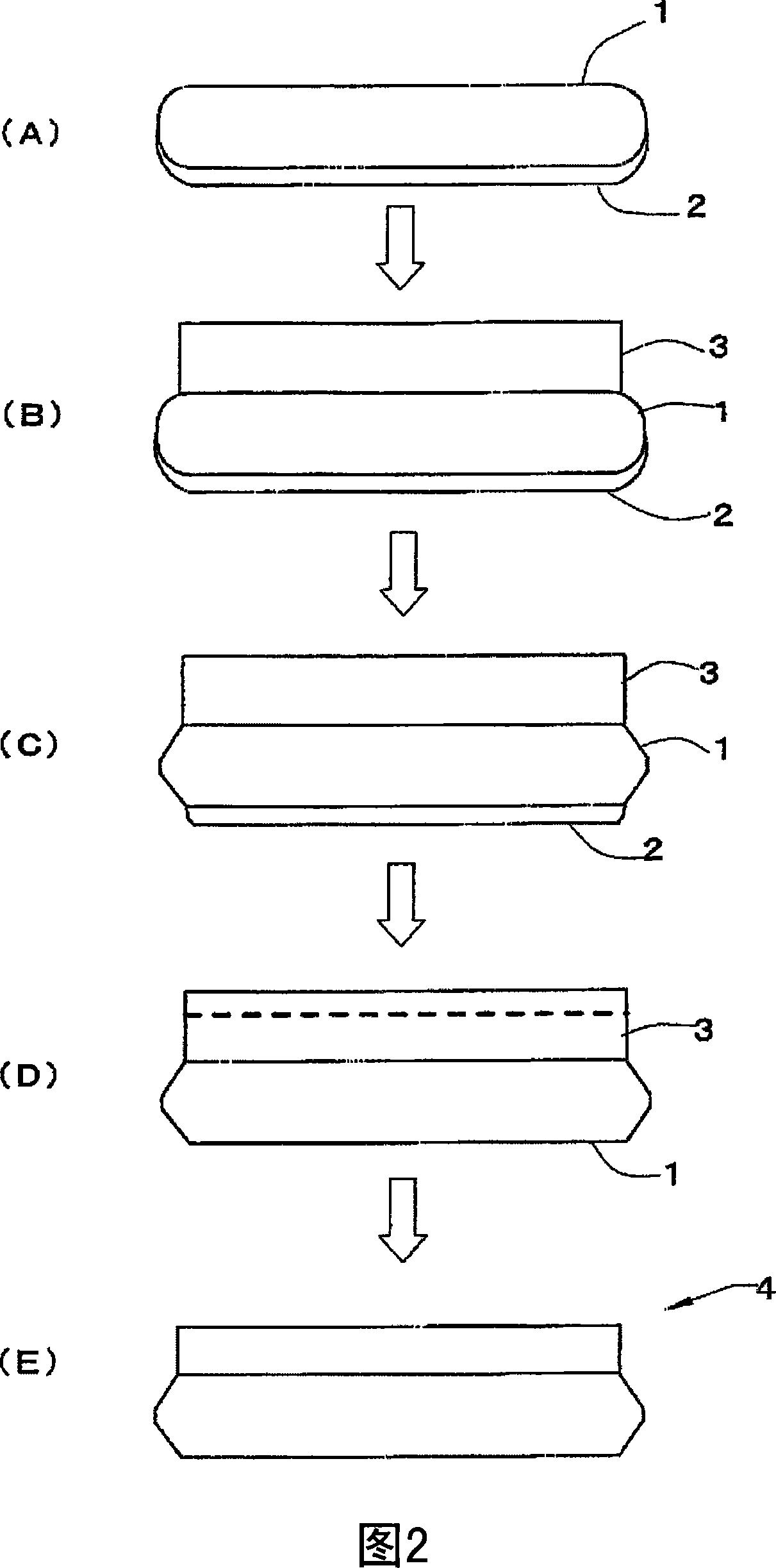
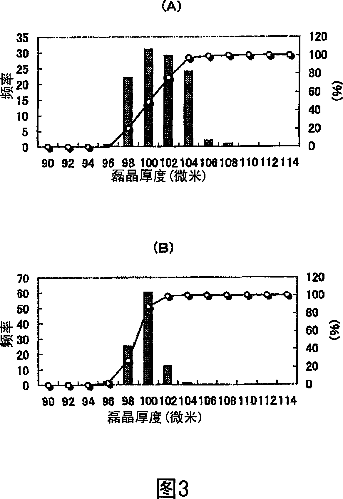
[0098] Prepare 200 silicon wafers with a diameter of 200 mm, a thickness specification of 625 μm, a P type, a resistivity of 5 to 10 mΩcm, and a TTV (flatness specification) of 2.0 μm or less as substrates for epitaxy. An oxide film (SiO 2 ). In addition, the thickness (initial thickness) of each wafer was measured before forming the CVD oxide film, and an ID number was added to each wafer by laser marking.

[0099] Epitaxial growth is a vertical epitaxial growth device that uses high-frequency heating. The epitaxial growth thickness is 120 microns as the target, the source gas is trichlorosilane, and the carrier gas is H 2 Gas, adjust the supply rate of trichlorosilane so that the growth rate is 4 μm / min. The epitaxial growth temperature (pedestal temperature) was set at 170°C. Also, the resistivity of the target epitaxial layer is N-type, 30Ωcm.

[0100] In addition, in order to suppress the bridge connection during epitaxial growth, a base is used, the base is formed w...


PUM

PropertyMeasurementUnit
thicknessaaaaaaaaaa
surface smoothnessaaaaaaaaaa
thicknessaaaaaaaaaa

Abstract

An epitaxial wafer manufacturing method at least includes a process (D) of growing an epitaxial layer thicker than a final target epitaxial layer on an epitaxial wafer having an initial thickness; a process (G) of planarizing the grown epitaxial layer by planarizing polishing; and a process (H) of polishing the epitaxial layer after the planarizing polishing. Preferably, a wafer having a TTV, which indicates planarity, of 2[mu]m or less is used as the epitaxial wafer, and further, the method includes an process (E) of grinding the chamfered part of the wafer and the process (E) of polishing the ground chamfered part. Thus, a technology of manufacturing the epitaxial wafer having excellent thickness uniformity of the epitaxial layer at a high productivity and low cost is provided, even when the epitaxial wafer is provided with the thick epitaxial layer.

Description

technical field [0001] The invention relates to an epitaxial wafer, in particular to a method for manufacturing an epitaxial wafer with a thicker epitaxial layer and less thickness deviation. Background technique [0002] In the manufacture of semiconductor devices, epitaxial wafers in which silicon single crystals are deposited on substrates such as silicon wafers are used. The epitaxial wafer can be manufactured according to the process shown in FIG. 6 , for example. First, an etched silicon wafer (CW) is prepared as a substrate for an epitaxial wafer. When using a wafer with a high doping concentration, a CVD oxide film is formed on the back side in order to prevent self-doping. Subsequently, the surface of the wafer (the surface on the side where the epitaxial layer is grown) is polished, and then washed. Subsequently, an epitaxial layer composed of a silicon single crystal is grown to a predetermined thickness on the polished surface of the substrate using an epitaxi...

Claims


Application Information

Patent Timeline
Patent Type & Authority Applications(China)
IPC IPC(8): H01L21/304H01L21/205
CPCH01L21/02008H01L21/3212H01L21/20H01L21/304
Inventor 高见泽彰一佐山隆司
Owner SHIN-ETSU HANDOTAI CO LTD
Why Eureka
Try Eureka