
Voltage clamping circuits using mos transistors and semiconductor chips and methods of clamping voltages

A clamping circuit, semiconductor technology, applied in the direction of logic circuit connection/interface layout, protection against damage caused by electrostatic discharge, pulse shaping, etc., can solve the problems of increasing the size of semiconductor chips, large design rules, and reducing the size of semiconductor chips

Active Publication Date: 2007-12-26
SAMSUNG ELECTRONICS CO LTD
View PDF1 Cites 5 Cited by
  • Summary
  • Abstract
  • Description
  • Claims
  • Application Information

AI Technical Summary

Problems solved by technology

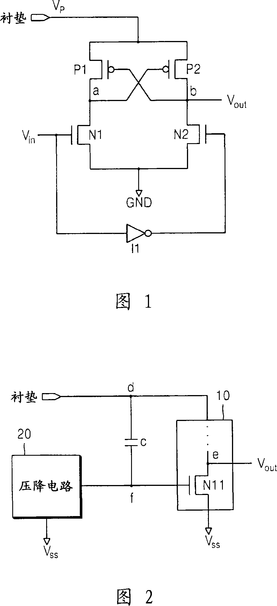
[0011] However, additional clamping circuits may increase the size of the semiconductor chip
Also, clamping circuits that clamp relatively high voltages generated by ESD may require large design rules, which may limit the size reduction of semiconductor chips

Method used


Image

  • Voltage clamping circuits using mos transistors and semiconductor chips and methods of clamping voltages
  • Voltage clamping circuits using mos transistors and semiconductor chips and methods of clamping voltages
  • Voltage clamping circuits using mos transistors and semiconductor chips and methods of clamping voltages

Examples


Embodiment Construction

[0030] Specific illustrative embodiments are disclosed herein. However, specific structural and functional details disclosed herein are for purposes of describing example embodiments only. The examples disclosed herein may, however, be embodied in many alternative forms and should not be construed as limited to the embodiments set forth herein.

[0031] Therefore, while there are many variations and alternative forms of the example embodiments, embodiments thereof are shown by way of example in the drawings and will be described in detail herein. It should be understood, however, that there is no intention to limit example embodiments to the particular forms disclosed, but on the contrary, example embodiments are to cover all modifications, equivalents, and alternatives falling within the scope of these embodiments. Like reference numerals refer to like elements throughout the description of the figures.

[0032] It will be understood that, although the terms first, second e...


PUM


Abstract

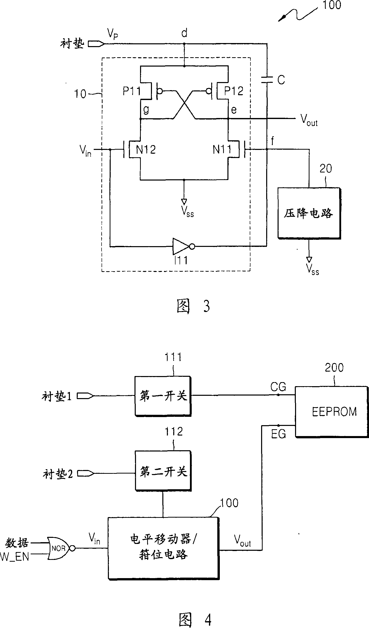
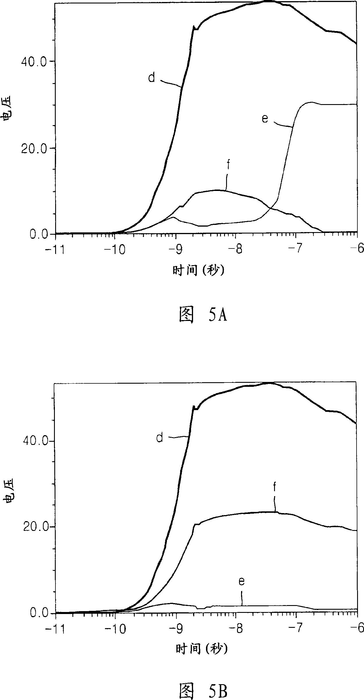
A clamping circuit is provided, which may clamp a voltage at a node of a circuit to a stable level by using a transistor already included in the circuit. The clamping circuit may clamp a voltage at a first node of a circuit inside a semiconductor chip to a more stable level when electro-static discharge (ESD) occurs. The clamping circuit may include a transistor and a capacitive element to store a control voltage to turn on the transistor in response to ESD.

Description

technical field [0001] Example embodiments may relate to circuits and / or semiconductor chips. For example, example embodiments may relate to voltage clamping circuits that may clamp voltages at nodes within circuits of a semiconductor chip. Example embodiments may include MOS transistors and / or semiconductor chips having the same. Background technique [0002] In the prior art, when a semiconductor chip is integrated, current may be introduced by wiring through the pad due to static electricity. This current may cause errors and / or damage the semiconductor chip. In order to protect circuits inside the semiconductor chip from electrostatic discharge (ESD) or the like, the semiconductor chip may include an ESD protection circuit. The ESD protection circuit may be arranged near a pad in the semiconductor chip and / or may be located between the pad and the circuitry of the semiconductor chip. Therefore, when a current generated by static electricity is introduced through the ...

Claims


Application Information

Patent Timeline
IPC IPC(8): H03K5/08
CPCH05K9/0067H03K19/0175
Inventor 任敬植金汉求高在赫孙日宪金锡震
Owner SAMSUNG ELECTRONICS CO LTD
Learn More