Full-automatic wafer rear marking machine

A marking machine, fully automatic technology, applied in the direction of conveyor objects, electrical components, semiconductor/solid-state device manufacturing, etc., can solve the problems of high equipment cost and material cost, slow marking speed, etc., to improve marking quality, The effect of faster opening speed and higher production efficiency

Inactive Publication Date: 2008-01-02
GRAND TECH SHENZHEN
View PDF0 Cites 23 Cited by
  • Summary
  • Abstract
  • Description
  • Claims
  • Application Information

AI Technical Summary

Problems solved by technology

[0004] The purpose of the present invention is to provide a new type of fully automatic wafer backside marking machine for the shortcomings of the existing wafer marking machine, such as slow marking speed, high equipment cost and high material cost.

Method used


Image

  • Full-automatic wafer rear marking machine
  • Full-automatic wafer rear marking machine
  • Full-automatic wafer rear marking machine

Examples


Embodiment Construction

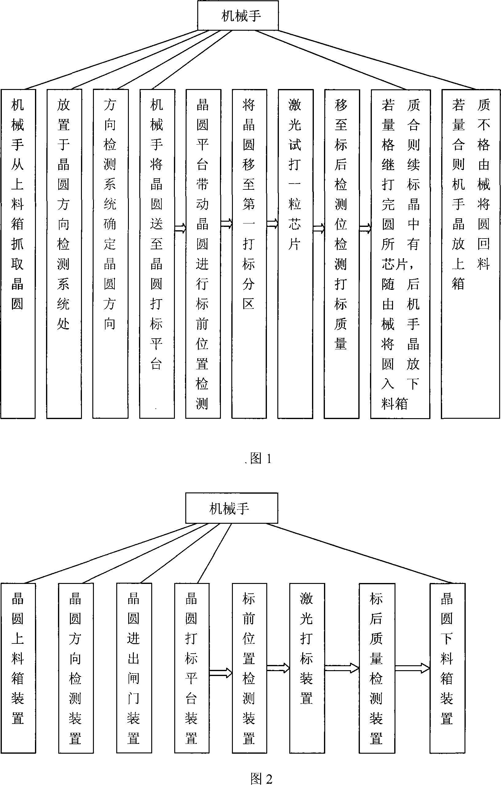
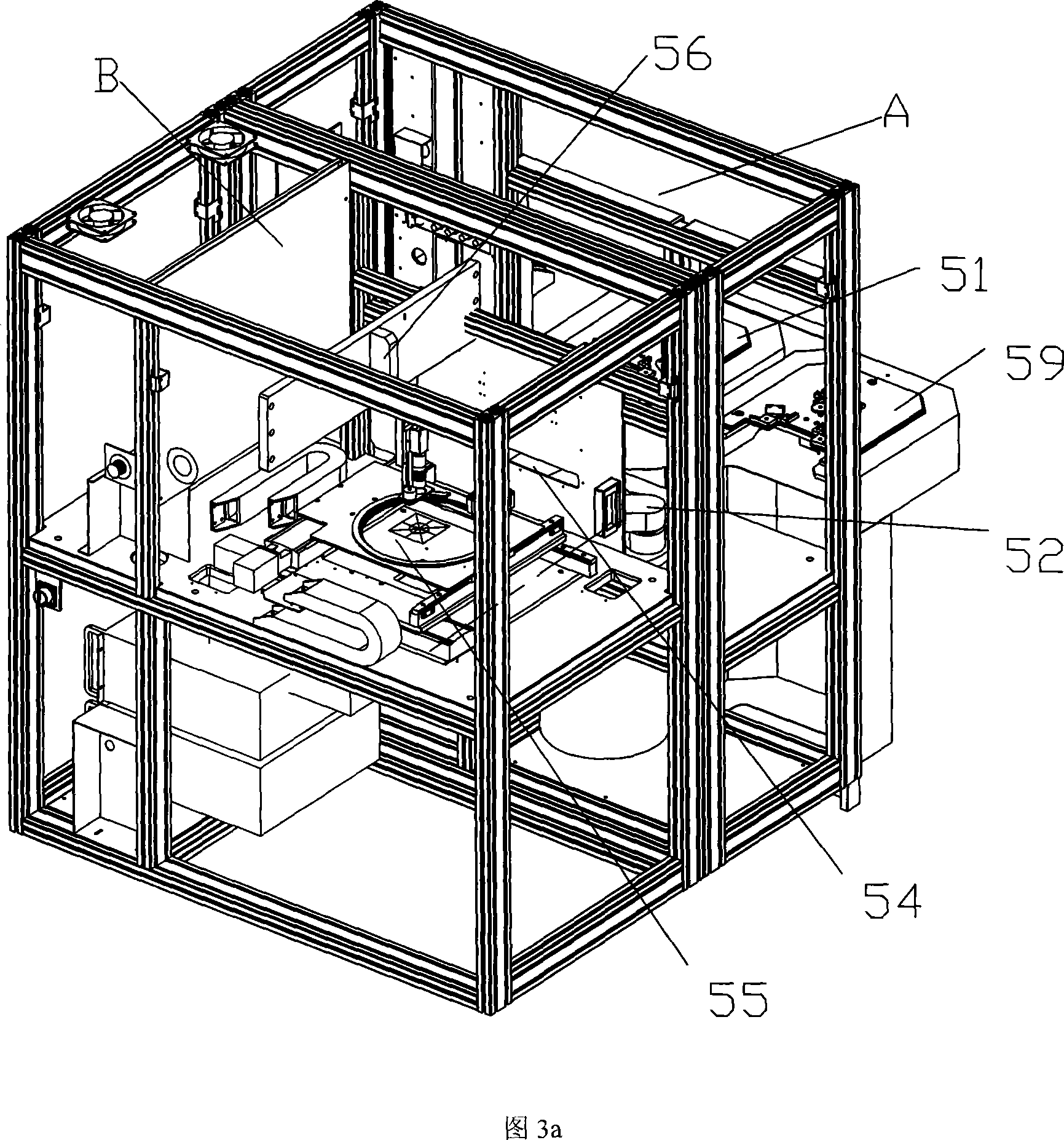
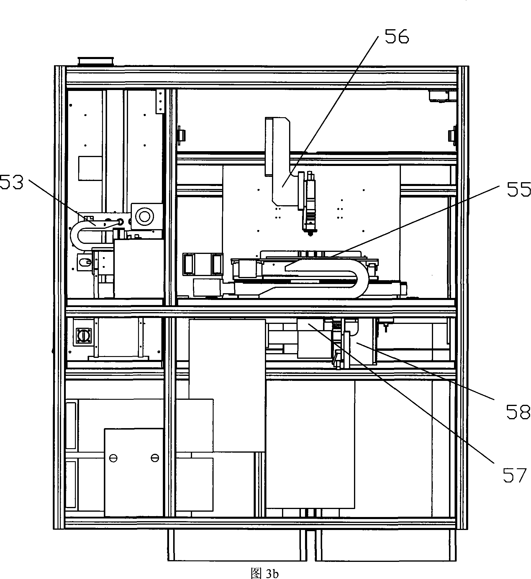
[0034] As shown in Figure 3a to Figure 3d, a fully automatic marking machine for the back of a wafer is composed of front and rear areas, wherein an electric control device 510 and a PC 511 are arranged on the front area, A partition is provided between the front area A and the rear area B, and a gate import and export device 54 is arranged on the partition, and an upper material box device 51 and a lower material box device 59 are arranged on the outside of the front area A, and the front area A A manipulator 52 and a wafer direction detection device 53 are provided inside the rear area; a wafer marking platform device 55 is provided inside the rear area, and a pre-marking detection device 56 and a post-marking detection device are respectively provided above and below the marking platform device 55 58.

[0035] As shown in Figures 4a to 4d, the described loading box device includes a box support frame 7, a box seat 6 installed on the box support frame 7, and a box cover 1 pl...


PUM


Abstract

The invention relates to a novel device for marking IC crystal, in particular to a full-automatic crystal back marking machine, which uses a mechanical hand to take out crystal from a material feeding box to be sent to a crystal direction checker, a crystal marking platform or the like, to be marked and checked to be taken off by a mechanical hand to be put into a material outputting box. The invention is composed of a front area and a back area, wherein the front area is arranged with an electric controller and a PC, a baffle plate is arranged between the front and back areas, the baffle plate is arranged with a gate entrance, the outer side of the front area is arranged with a material feeding box and a material discharging device, the front area is arranged with a mechanical hand and a crystal direction checker inside, the back area is arranged with a crystal marking platform inside, the marking platform is respectively arranged with a before-marking checker and an after-marking checker above and under.

Description

technical field [0001] The present invention relates to a new equipment for marking IC wafers. More precisely, it involves using a manipulator to take out the wafers from the loading box, and then send them one by one to the wafer direction detection device, wafer marking platform and other devices. After marking and testing, it is a fully automatic marking machine for the back of the wafer that is taken out by the manipulator and put into the unloading box. Background technique [0002] Marking machines are widely used in the surface marking of integrated circuits in the IC industry. According to the different requirements of use, the integrated circuit board used in the IC industry has three forms: strips, that is, combined chips; chips, that is, granular chips, hereinafter also referred to as materials and components; and wafers. The material bar is a sheet material composed of several chips. When marking each chip on the material bar, the automatic marking is realized d...

Claims


Application Information

Patent Timeline
Patent Type & Authority Applications(China)
IPC IPC(8): H01L21/00H01L21/67H01L21/677
Inventor 陈有章林宜龙唐召来张松岭冀守恒
Owner GRAND TECH SHENZHEN
Why Eureka
Try Eureka