Peeling method, semiconductor device, and manufacturing method therefor
A semiconductor and device technology, which is applied in the field of peeling off the peeling layer, can solve the problems that it is difficult to prepare a transmissive liquid crystal display device, it is difficult to peel off the peeling layer, etc.
- Summary
- Abstract
- Description
- Claims
- Application Information
AI Technical Summary
Problems solved by technology
Method used
Image

Examples
Embodiment 1
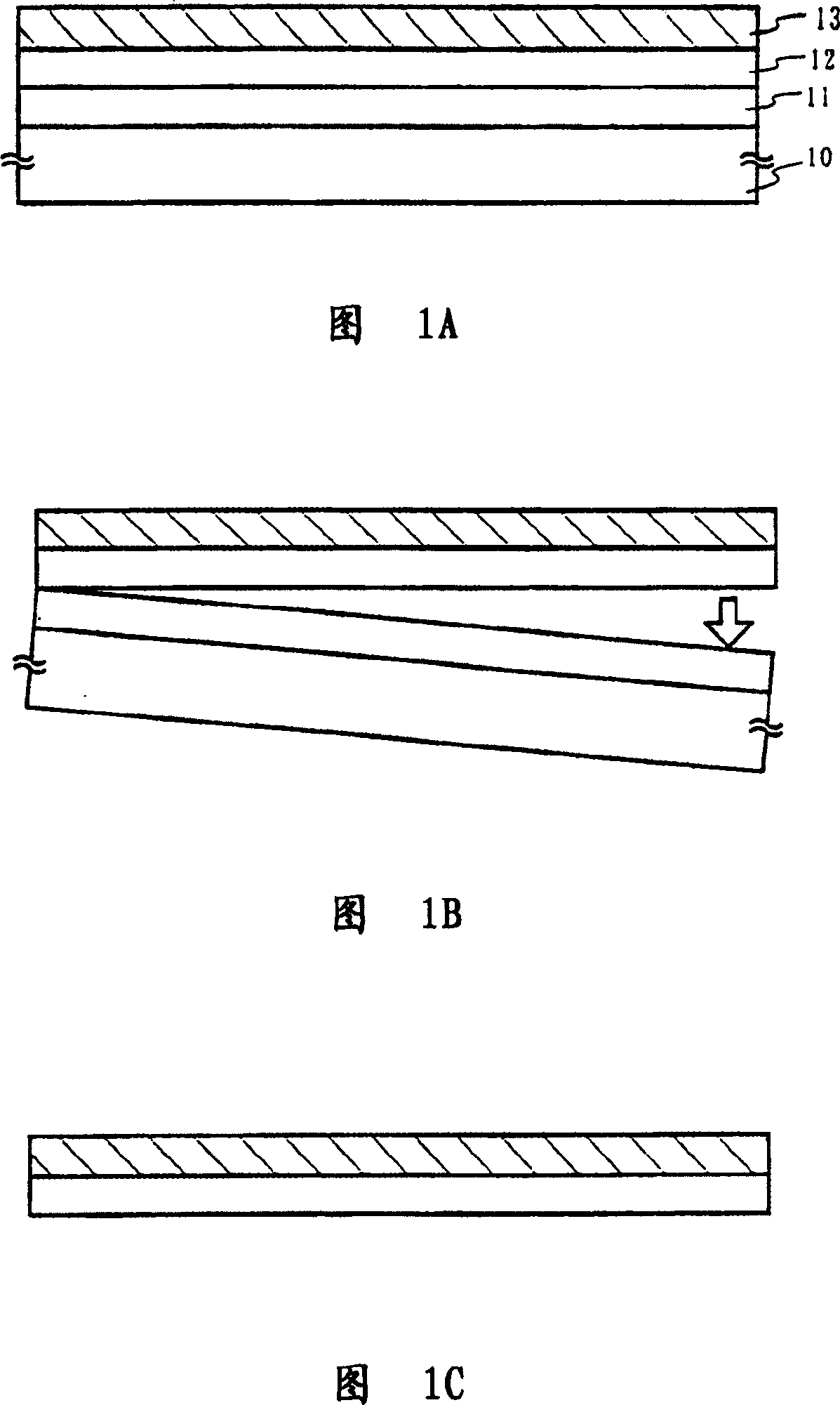
[0151] Here, a representative exfoliation process utilizing the present invention is schematically shown in FIG. 1 .
[0152] In FIG. 1A, reference numeral 10 denotes a substrate, reference numeral 11 denotes a nitride layer or a metal layer, reference numeral 12 denotes an oxide layer, and reference numeral 13 denotes a lift-off layer.
[0153] In FIG. 1A, for the substrate 10, a glass substrate, a quartz substrate, a ceramic substrate, or the like can be used. In addition, a silicon substrate, a metal substrate, or a stainless steel substrate may also be used.
[0154] First, as shown in FIG. 1A, a nitride layer or metal layer 11 is formed on a substrate 10. Referring to FIG. For the nitride layer or metal layer 11, representative examples are as follows: selected from Ti, Al, Ta, W, Mo, Cu, Cr, Nd, Fe, Ni, Co, Zr, Zn, Ru, Rh, Pd, Os , an element in Ir and Pt, or a single layer composed of alloy materials or compound materials whose main components are the above elements, ...
Embodiment 2
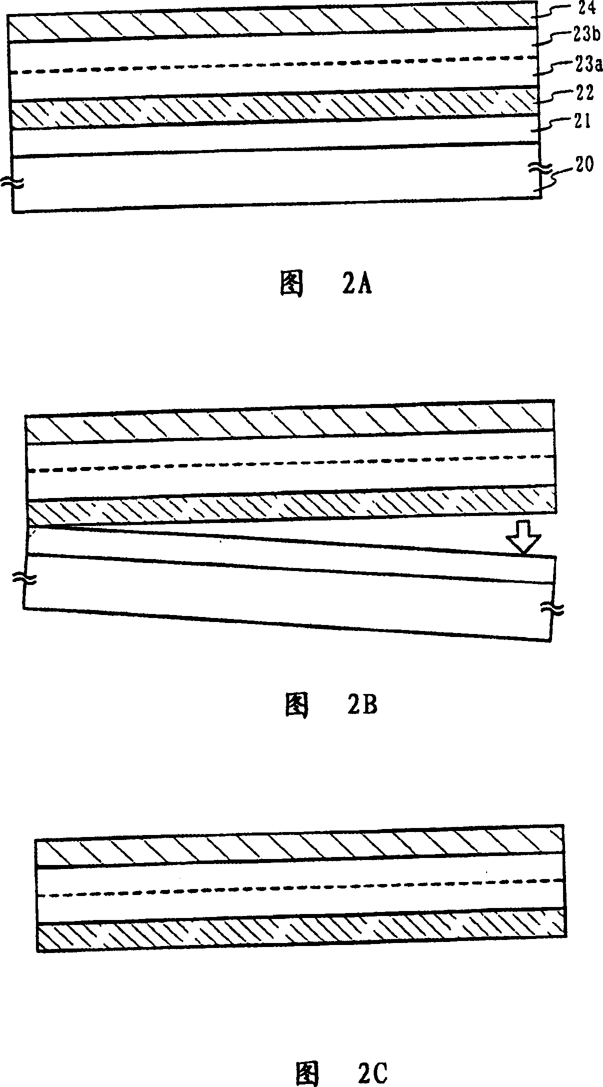
[0160] For this embodiment, the stripping process in which the substrate is stripped away while preventing the diffusion of impurities from the nitride layer or metal layer and the substrate by providing an initial capping insulating layer in contact with the stripping layer is schematically shown in FIG. 2 . In FIG. 2A, reference numeral 20 denotes a substrate, reference numeral 21 denotes a nitride layer or a metal layer, reference numeral 22 denotes an oxide layer, reference numerals and characters 23a and 23b denote an initial covering insulating layer, and reference numeral 24 denotes a peeling layer.
[0161] In FIG. 2A, for the substrate 20, a glass substrate, a quartz substrate, a ceramic substrate, or the like can be used. In addition, a silicon substrate, a metal substrate, or a stainless steel substrate may also be used.
[0162] First, a nitride layer or metal layer 21 is formed on a substrate 20 as shown in FIG. 1A. For the nitride layer or metal layer 21, repres...
Embodiment 3
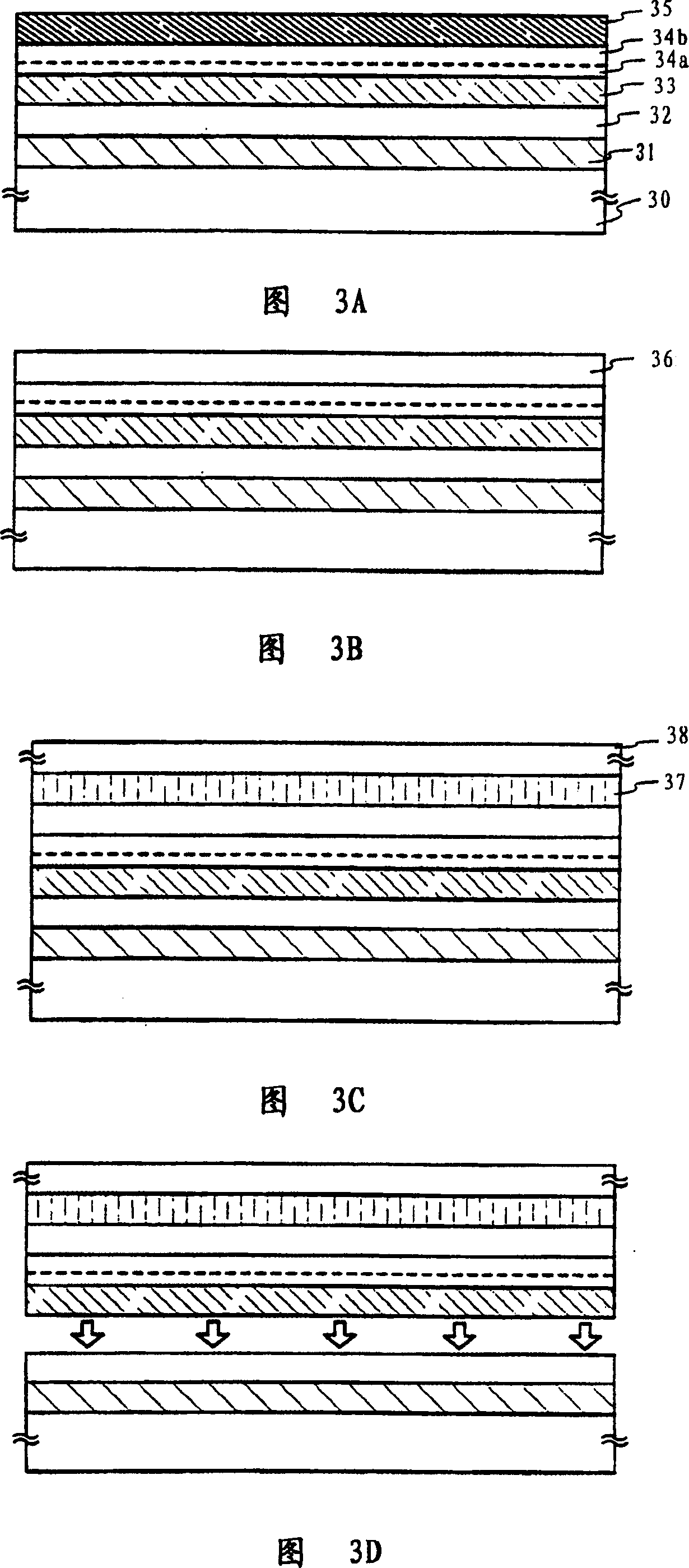
[0172] In this example, in addition to Example 1, an example of performing laser beam irradiation or heat treatment to promote peeling is shown in FIG. 4 .
[0173] In FIG. 4A, reference numeral 40 denotes a substrate, reference numeral 41 denotes a nitride layer or a metal layer, reference numeral 42 denotes an oxide layer, and reference numeral 43 denotes a lift-off layer.
[0174] Since the steps of forming it up to preparation of the peeling layer are the same as in Example 1, the description is omitted.
[0175] After the release layer was formed, laser beam irradiation was performed (FIG. 3A). For the laser beam, a gas laser such as an excimer laser or the like, a solid-state laser such as a YVO4 laser, a YAG laser or the like, and a semiconductor laser can be used. In addition, the form of laser light can be continuous oscillation or pulse oscillation, and the shape of the laser beam can be any one of straight line, rectangle, circle or ellipse. Furthermore, the wavel...
PUM
| Property | Measurement | Unit |
|---|---|---|
| Thickness | aaaaa | aaaaa |
| Thickness | aaaaa | aaaaa |
| Thickness | aaaaa | aaaaa |
Abstract
Description
Claims
Application Information
PatSnap Eureka turns technology decisions into work you can execute. Powered by our Innovation Knowledge Graph, it runs expert workflows across engineering, life sciences, materials and intellectual property. Get your review-ready output in minutes.


