Three-dimensional on-line measuring method and system using synthesis wave to interfere whole-field nano surface

A measurement system and measurement method technology, applied in the field of optical measurement, can solve problems such as complex scanning mechanism, high instrument cost, and slow measurement speed, and achieve the effects of simple system structure, high measurement accuracy, and fast measurement speed

Inactive Publication Date: 2008-01-23
BEIJING JIAOTONG UNIV
View PDF0 Cites 4 Cited by
  • Summary
  • Abstract
  • Description
  • Claims
  • Application Information

AI Technical Summary

Problems solved by technology

[0009] 1. They are all point scanning measurement methods, the measurement speed is slow, two-dimensional scanning is required for three-dimensional surface measurement, the scanning mechanism is complicated, and the instrument cost is high;
[0010] 2. It is sensitive to interference such as measurement environment vibration and temperature drift, and is not suitable for online measurement;
[0011] 3. The measurement range is limited by the wavelength λ of the incident light wave, the measurement range is less than λ / 2, and it is impossible to measure the nano-surface with the boss and deep groove structure

Method used


Image

  • Three-dimensional on-line measuring method and system using synthesis wave to interfere whole-field nano surface
  • Three-dimensional on-line measuring method and system using synthesis wave to interfere whole-field nano surface
  • Three-dimensional on-line measuring method and system using synthesis wave to interfere whole-field nano surface

Examples


Embodiment Construction

[0024] The present invention will be further described below in conjunction with the accompanying drawings and specific embodiments.

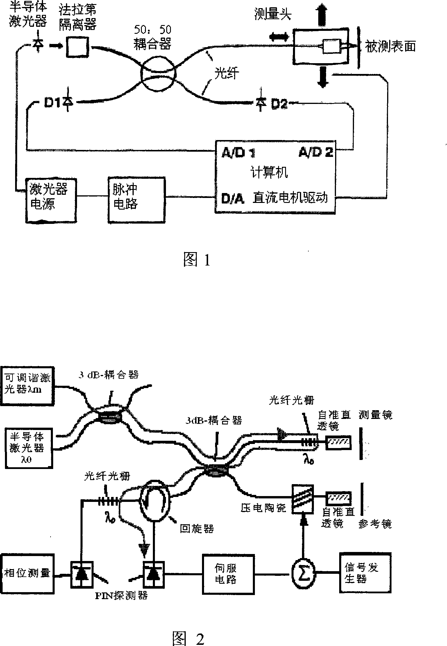
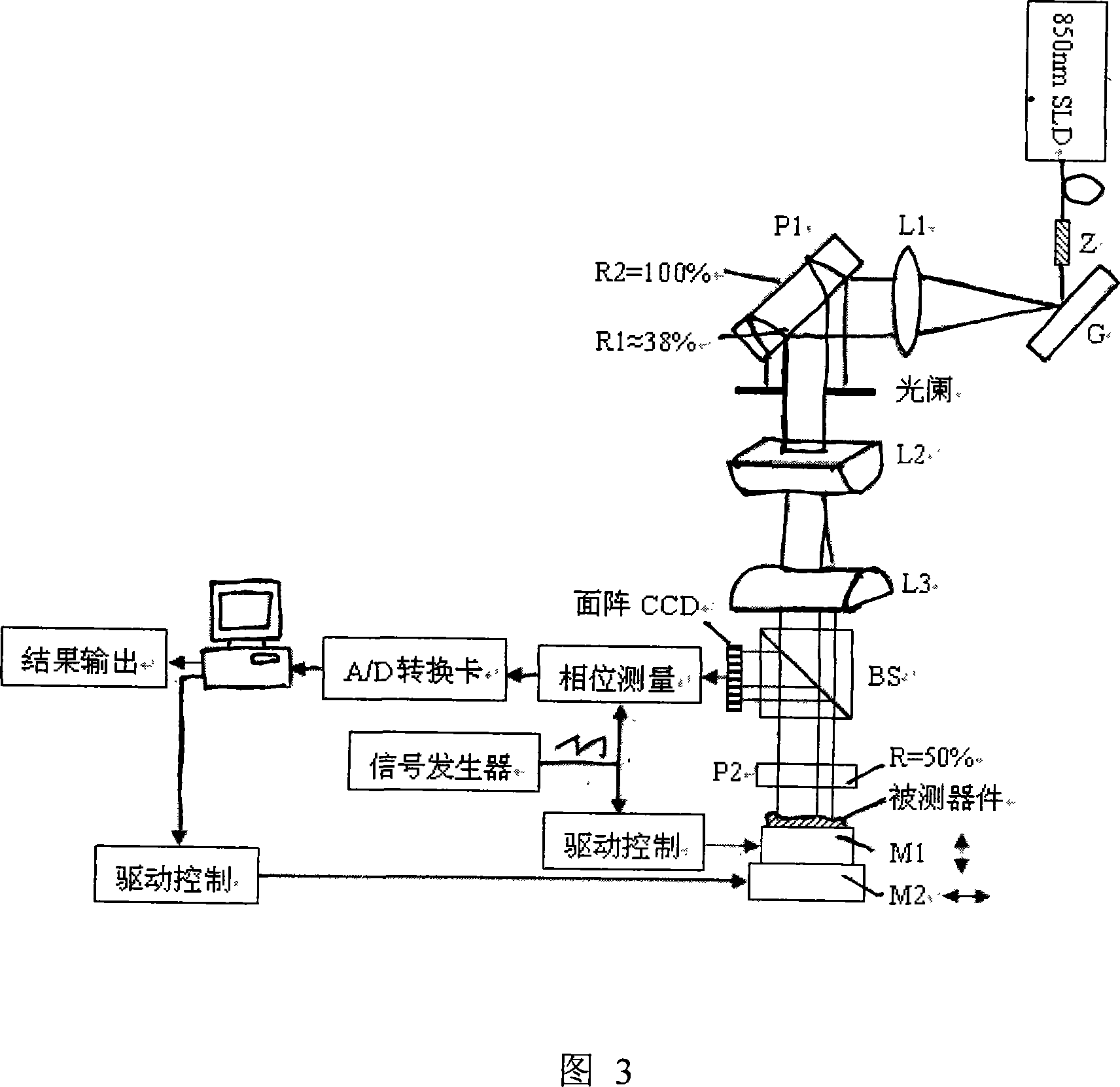
[0025] As shown in Figure 3, the light with a spectral width of 40nm emitted by a superluminescent diode SLD with a center wavelength of 850nm is collimated into a parallel beam after passing through the fiber self-collimating lens Z, and the parallel beam is dispersed by the grating G to become a continuous and uniform wavelength in space Distributed fan-shaped light sheet, this fan-shaped light sheet is collimated into a parallel light sheet with continuous and uniform distribution of wavelength in space after passing through the collimating lens L1, and the parallel light sheet is obliquely incident on the parallel glass plate P1 with the thickness d of the coating on both sides, parallel The upper surface of the glass plate P1 is coated with a partial reflective film, and the lower surface is coated with a reflective film with a reflectivity...


PUM


Abstract

The invention provides a nanometer surface 3D on-line measuring method by using composed wave to interfere the whole field and a system for the method. The measuring range is depending upon the composed wavelength and co-path interference structure. The grating scatters the light beam of spectrum width 40 nm into two segment light pieces with wavelengths continuously and evenly distributed in the space, which are collimated into two parallel light pieces that are staggered in cross direction and are partially overlapped; the overlapped part forms the composed wave. The beam of the parallel light pieces of the composed wave is expanded by two co-focus plane cylinder lens, then through a parallel glass plate, one surface of which is coated with a semi-permeable and half-reflecting membrane, half light intensity is reflected as reference light, another half light intensity is reflected by different measured points, and is detected by a planar array CCD after being interfered by the reference light. Once the phase change of the interference signal for each pixel of CCD is measured, the longitudinal change of the measured point is got. 3D measurements for the surface is completed in one positioning. The measurement is of high speed and low cost. The measuring range is 600 swung dash 1000 Mu m, the resolution is better than 5 nm, is applicable for 3D measuring for nanometer surfaces with bosses and deep slots.

Description

technical field [0001] The invention relates to a method and system for three-dimensional on-line measurement of nano-surfaces using synthetic wave interference, in particular to a method and system for three-dimensional on-line measurement of nano-surfaces with boss and deep groove structures, belonging to the technical field of optical measurement. Background technique [0002] [1] D.P. Hand, T.A. Carolan, J.S. Barton, and J.D.C. Jones, Optics Letters, 1993, Vol. 18, No. 16, pp. 1361-1363. The working principle of the prior art document [1] is shown in Figure 1. The light emitted by the semiconductor laser passes through the Faraday isolator and the optical fiber 50:50 coupler, and then reaches the measuring head. The measuring head is a Fizeau interferometer, and a part of the light is The reflection of the end face of the fiber is used as the reference light, and the other part of the light is projected onto the measured surface after being focused by the self-focusing l...

Claims


Application Information

Patent Timeline
IPC IPC(8): G01B11/00G01B11/03G01B9/02G02B27/00
Inventor 谢芳张琳
Owner BEIJING JIAOTONG UNIV
Why Eureka
Try Eureka