Multi-layer printed wiring board and manufacturing method thereof

A multi-layer printing, circuit board technology, applied in the directions of printed circuits, printed circuits, printed circuit manufacturing, etc., can solve the problems of peeling, easy cracking, poor ductility, etc.

Inactive Publication Date: 2008-01-23
IBIDEN CO LTD
View PDF2 Cites 7 Cited by
  • Summary
  • Abstract
  • Description
  • Claims
  • Application Information

AI Technical Summary

Problems solved by technology

It is generally believed that because the electroless plating film formed earlier contains organic matter, hydrogen molecules, hydrogen atoms, etc. and is relatively brittle, cracks are likely to occur on the electroless plating film.
In addition, it is generally believed that since the ductility of the electroless plating film is poor, when a warpage occurs on the printed wiring board when mounting an IC chip or the like, the electroless plating film cannot follow the warpage. Deformed and easy to peel off the land

Method used


Image

  • Multi-layer printed wiring board and manufacturing method thereof
  • Multi-layer printed wiring board and manufacturing method thereof
  • Multi-layer printed wiring board and manufacturing method thereof

Examples


no. 1 Embodiment

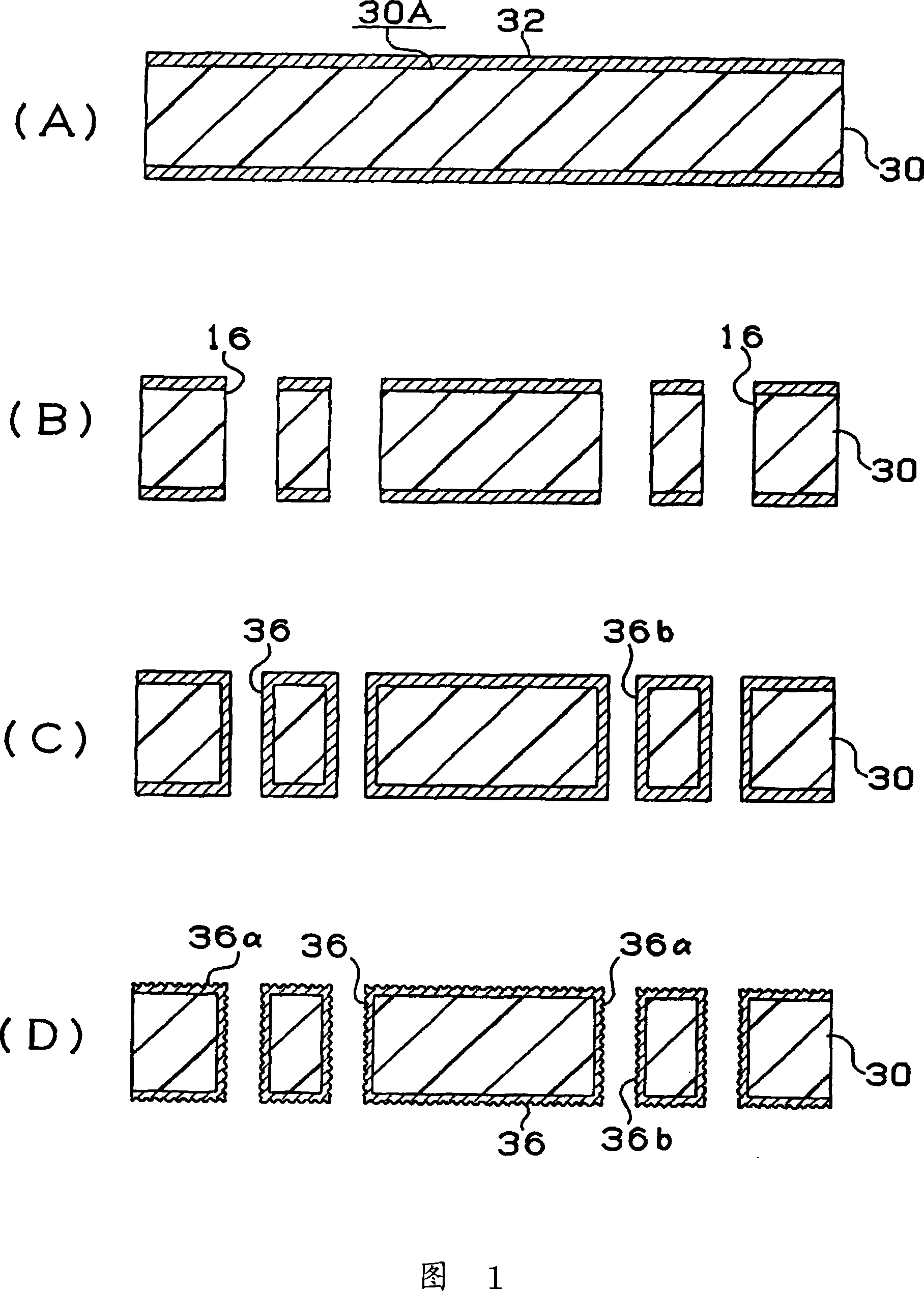
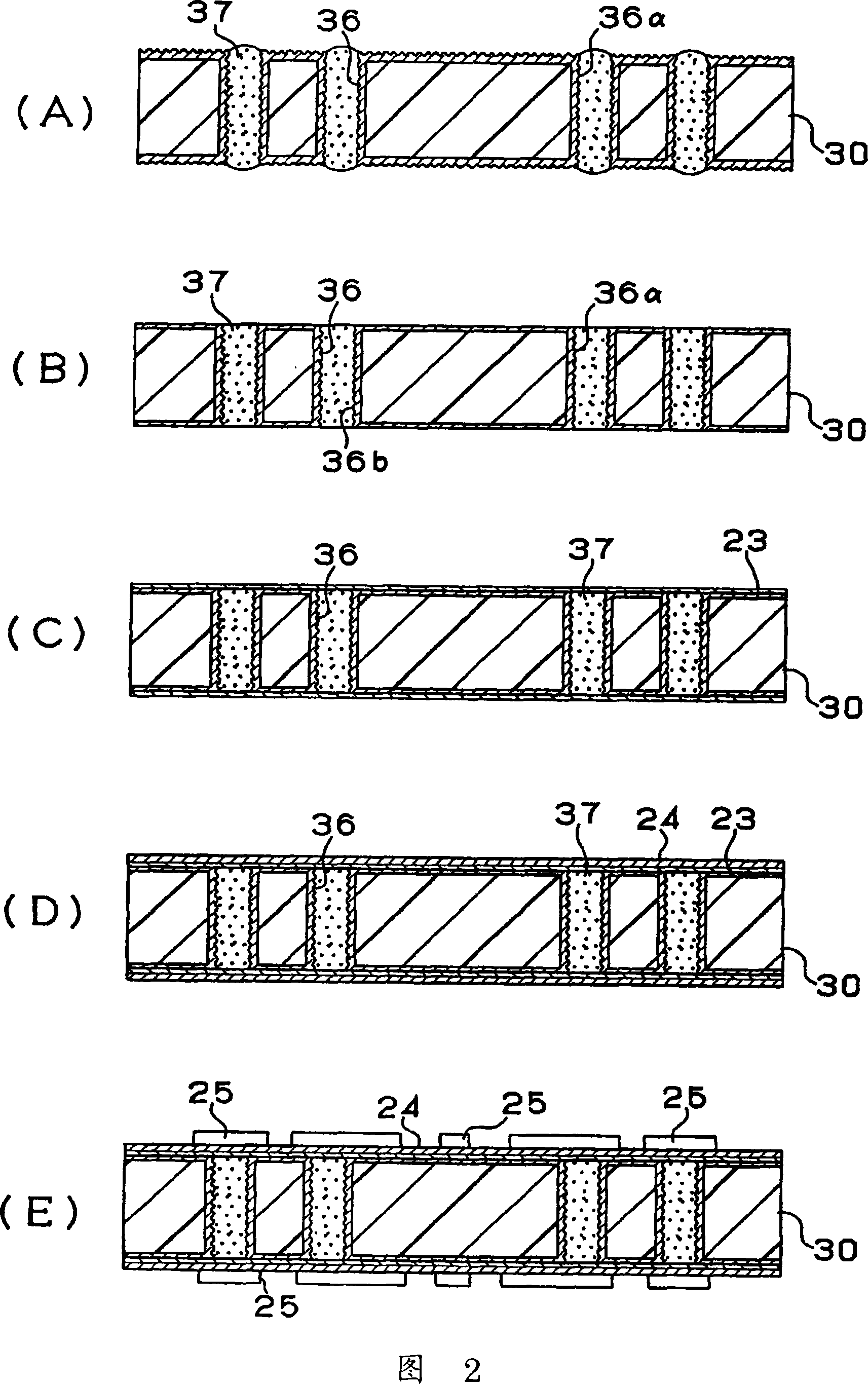
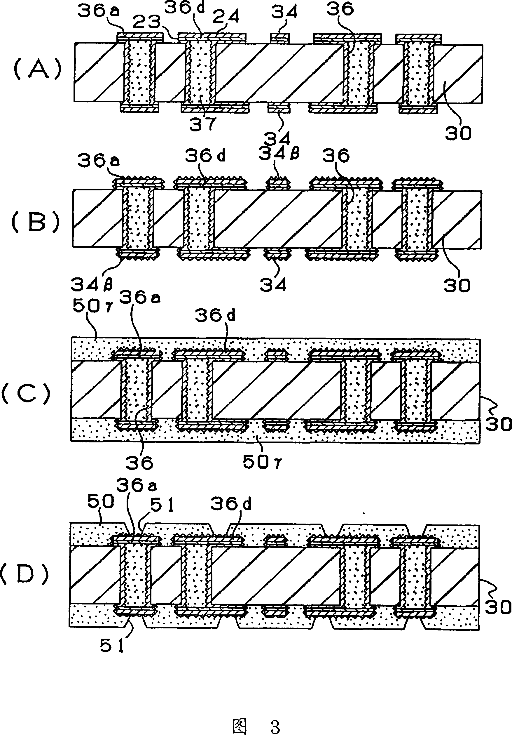
[0035] First, the structure of a multilayer printed wiring board 10 according to a first embodiment of the present invention will be described with reference to FIGS. 1 to 8 . FIG. 7 shows a cross-sectional view of the multilayer printed wiring board 10, and FIG. 8 shows a process of mounting an IC chip 90 on the multilayer printed wiring board 10 shown in FIG. state. As shown in FIG. 7 , in the multilayer printed wiring board 10 , a conductor circuit 34 is formed on the surface of the core substrate 30 . The front and back surfaces of the core substrate 30 are connected by through holes 36 . The through hole 36 is composed of cap-shaped plating layers 36a, 36d constituting a via land, and a sidewall conductor layer 36b, and the inside of the sidewall conductor layer 36b is filled with a resin filling material 37. The interlaminar resin insulating layer 50 and the interlaminar resin insulating layer 150 are disposed on the cap-shaped plating layers (via lands) 36a and 36d. ...


PUM

PropertyMeasurementUnit
thicknessaaaaaaaaaa
thicknessaaaaaaaaaa
current densityaaaaaaaaaa

Abstract

[Problems] To provide a multi-layer printed wiring board without decrease in connection reliability by forming a filled via right above a filled via of a small radius. [Means of Solving the Problems] During a heat cycle, the stress applied to a filled via 60 formed on cover plated layers 36a and 36d is larger than the stress applied to a filled via 160 formed on the second interlayer resin insulation layer 150. Therefore, the bottom diameter d 1 of the filled via 60 is made larger than the bottom diameter d2 of the filled via 160 formed right above the filled via 60.

Description

technical field [0001] The present invention relates to a multilayer printed wiring board, and in particular to a laminated multilayer printed wiring board suitable for use as a package substrate for IC chip mounting. Background technique [0002] In a build-up multilayer printed wiring board constituting a package for an IC chip, an interlayer insulating resin is formed on both sides or one side of a core substrate in which a through-hole is formed by drilling, and is opened by laser or photolithography. A via hole for conducting interlayer conduction forms an interlayer resin insulating layer. On the inner wall of the via hole, a conductive layer is formed by plating or the like, and patterned by etching or the like to produce a conductive circuit. Furthermore, by repeating the operation of forming the interlayer insulating layer and the conductor layer, a build-up multilayer printed wiring board is obtained. In the latest build-up multilayer circuit board, in order to i...

Claims


Application Information

Patent Timeline
Patent Type & Authority Applications(China)
IPC IPC(8): H05K3/46H01R12/51
CPCH05K3/4602H05K2201/09563H05K2201/09627H05K2201/0959H05K2201/0352H05K2201/0347H05K1/115H05K2201/096H05K2201/09454Y10T29/49155Y10T29/49165Y10T29/49147H05K3/46
Inventor 吴有红
Owner IBIDEN CO LTD
Why Eureka
Try Eureka