Multilayer printed wiring board
A multi-layer printing and circuit board technology, applied in the direction of printed circuit, printed circuit, printed circuit manufacturing, etc., can solve the problems of peeling, poor ductility, easy to produce cracks, etc., and achieve the effect of improving the integration rate
- Summary
- Abstract
- Description
- Claims
- Application Information
AI Technical Summary
Problems solved by technology
Method used
Image
Examples
no. 1 Embodiment
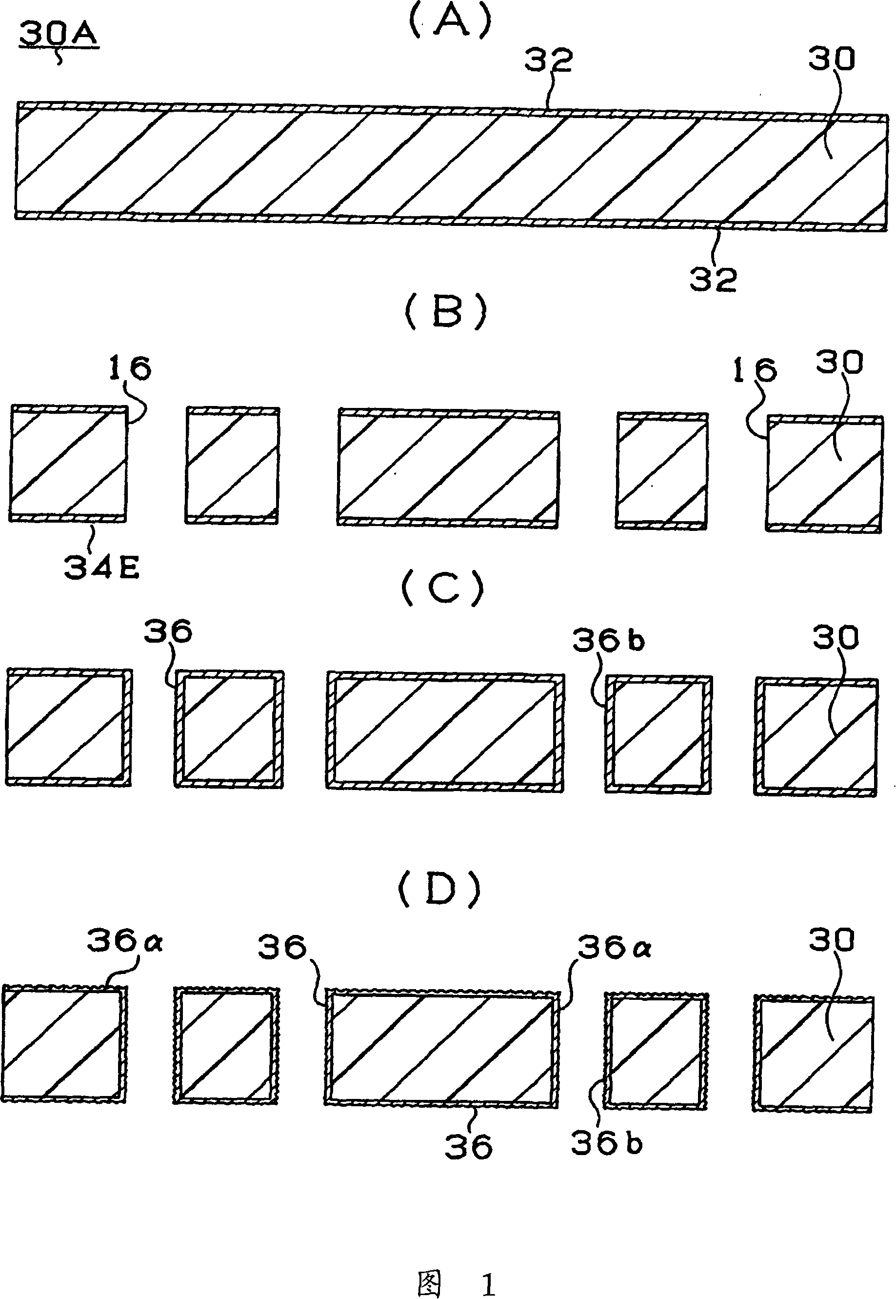
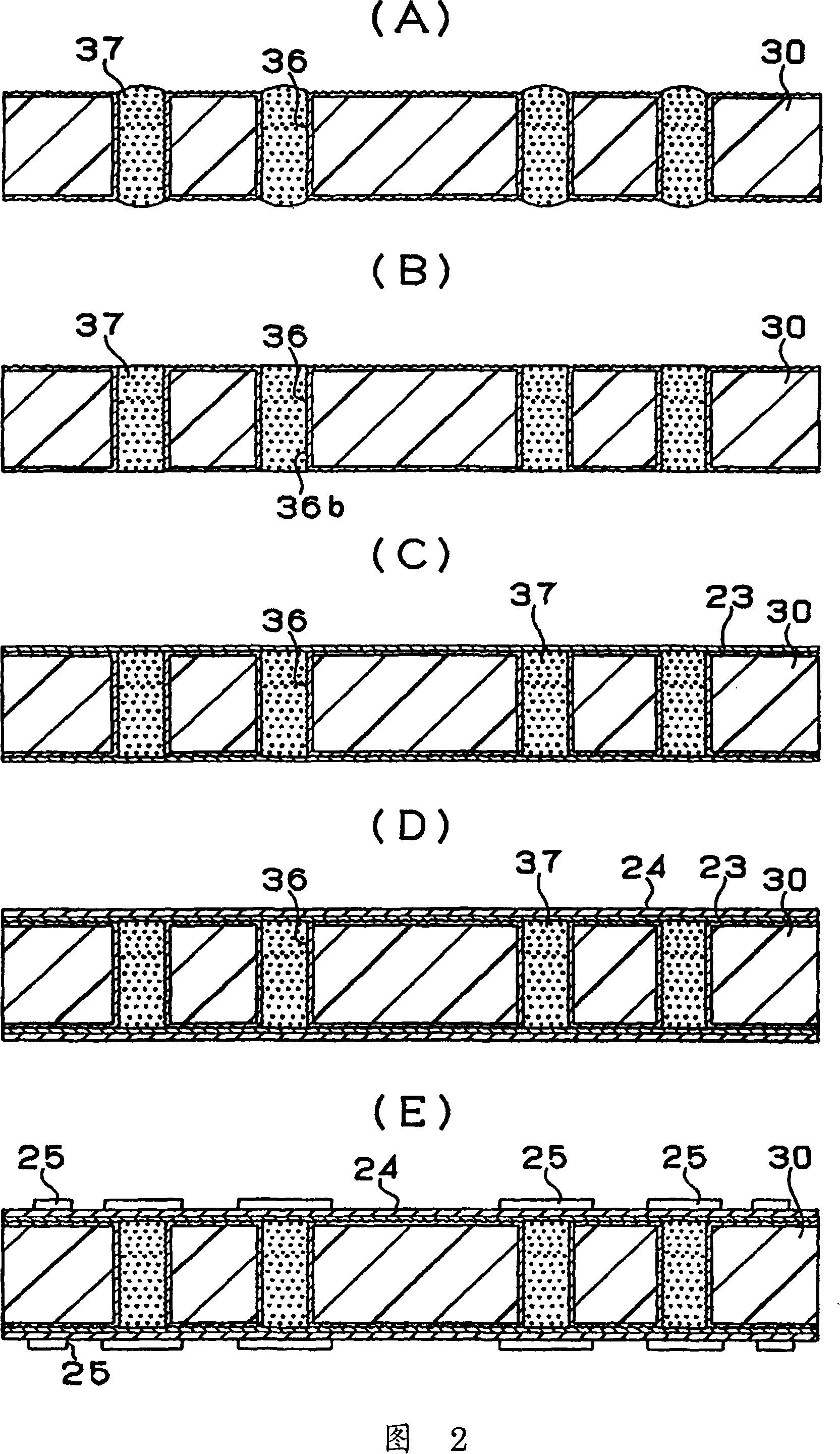
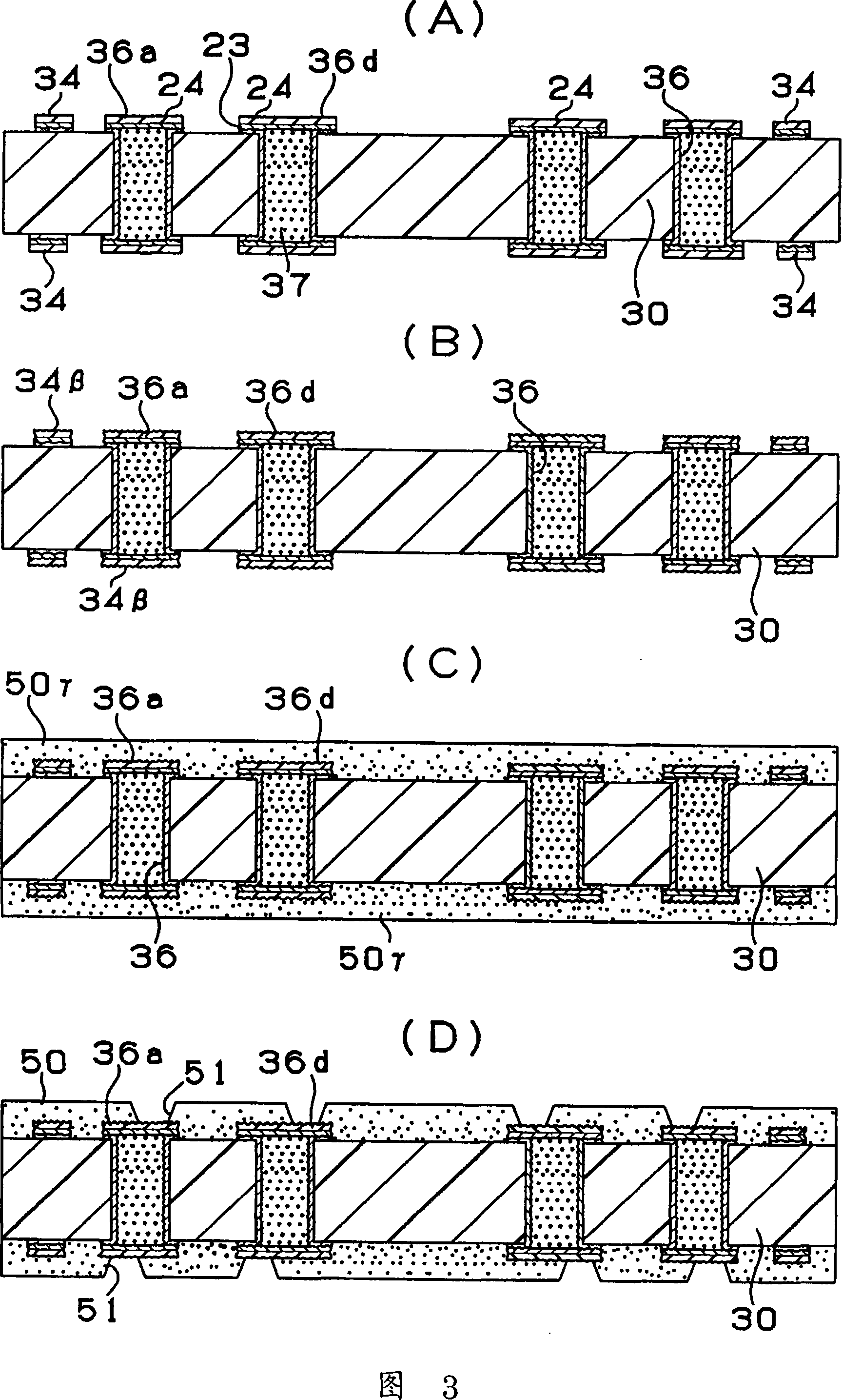
[0053]First, the structure of a multilayer printed wiring board 10 according to a first embodiment of the present invention will be described with reference to FIGS. 1 to 8 . FIG. 7 shows a cross-sectional view of the multilayer printed wiring board 10, and FIG. 8 shows a process of mounting an IC chip 90 on the multilayer printed wiring board 10 shown in FIG. state. As shown in FIG. 7 , in the multilayer printed wiring board 10 , a conductor circuit 34 is formed on the surface of the core substrate 30 . The front and back surfaces of the core substrate 30 are connected by through holes 36 . The through hole 36 is composed of cap-shaped plating layers 36a, 36d constituting a via land, and a sidewall conductor layer 36b, and the inside of the sidewall conductor layer 36b is filled with a resin filling material 37. It is also possible to fill only copper without using a resin filler. The interlaminar resin insulating layer 50 and the interlaminar resin insulating layer 150 ar...
no. 2 Embodiment
[0115] First, the structure of a multilayer printed wiring board 10 according to a second embodiment of the present invention will be described with reference to FIGS. 16 and 17 . FIG. 16 shows a sectional view of the multilayer printed wiring board 10, and FIG. 17 shows a process in which an IC chip 90 is mounted on the multilayer printed wiring board 10 shown in FIG. state. As shown in FIG. 16 , in the multilayer printed wiring board 10 , a conductor circuit 34 is formed on the surface of the core substrate 30 . The front and back surfaces of the core substrate 30 are connected by through holes 36 . The through hole 36 is composed of cap-shaped plating layers 36a, 36d constituting a via land, and a sidewall conductor layer 36b, and the inside of the sidewall conductor layer 36b is filled with a resin filling material 37. The interlaminar resin insulating layer 50 and the interlaminar resin insulating layer 150 are disposed on the cap-shaped plating layers (via lands) 36a a...
PUM
 Abstract
Description
Claims
Application Information


