
Microlenses of cmos image sensor and method for fabricating the same

A pattern and transparent layer technology, applied in the microlens of CMOS image sensor and its manufacturing field, can solve the problems of limiting the reproducibility of microlens, standardization of microlens focal length, standardization of difficult reflow processing, etc., to achieve optimal reproducibility and minimum crosstalk personalized, precise control of the effect

Inactive Publication Date: 2008-02-06
DONGBU HITEK CO LTD
View PDF1 Cites 3 Cited by
  • Summary
  • Abstract
  • Description
  • Claims
  • Application Information

AI Technical Summary

Problems solved by technology

Difficulty standardizing microlens focal lengths due to variations in the manufacturing process, limiting microlens reproducibility
For example, it is difficult to standardize reflow processing

Method used


Image

  • Microlenses of cmos image sensor and method for fabricating the same
  • Microlenses of cmos image sensor and method for fabricating the same
  • Microlenses of cmos image sensor and method for fabricating the same

Examples


Embodiment Construction

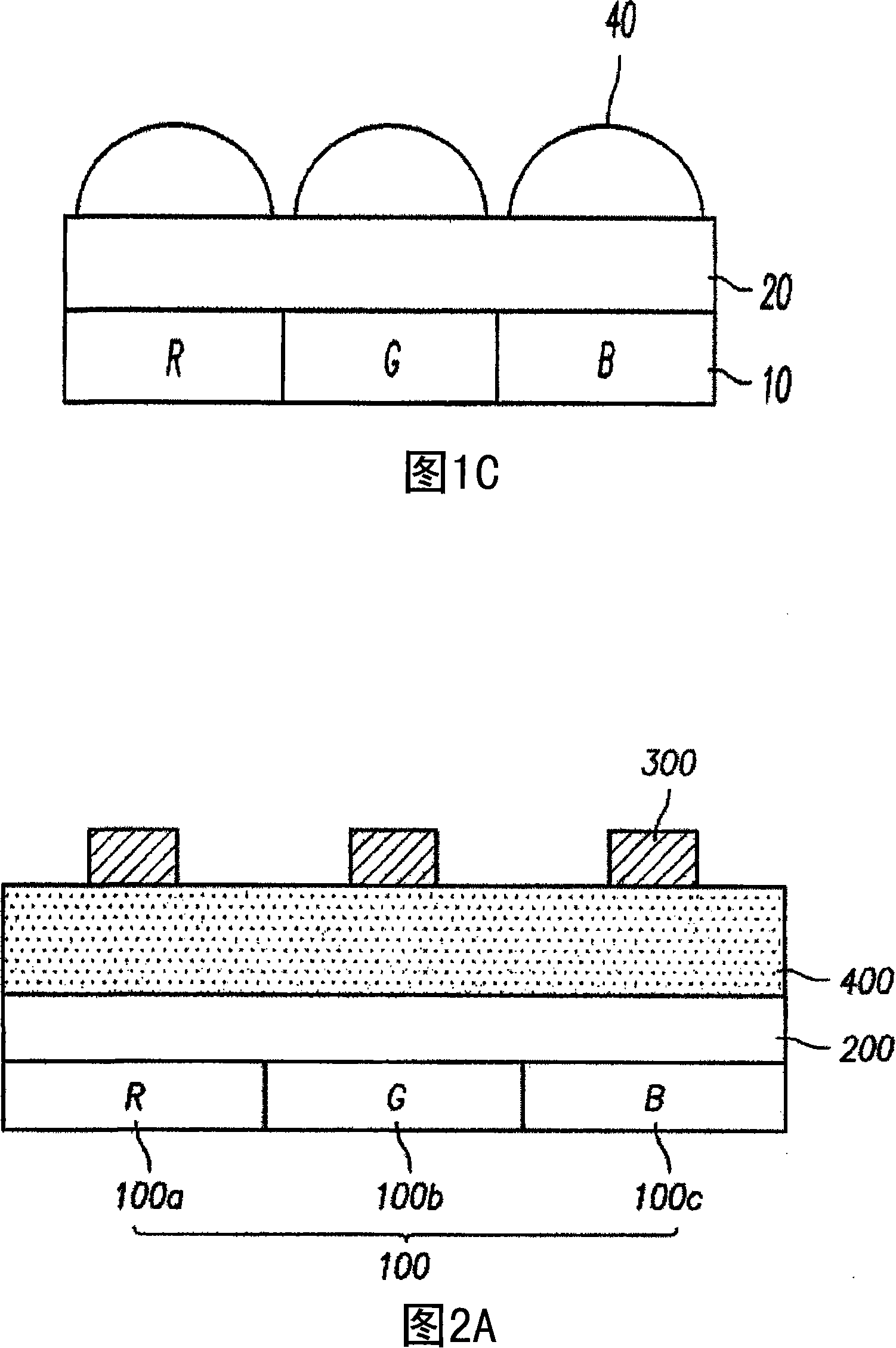
[0017] As shown in FIG. 2A , according to embodiments, color filter array 100 and / or planarization layer 200 are formed on and / or over a semiconductor substrate.

[0018] Silicon oxide (SiO 2 ) layer 400 is formed on and / or over planarization layer 200 and / or color filter array 100 .

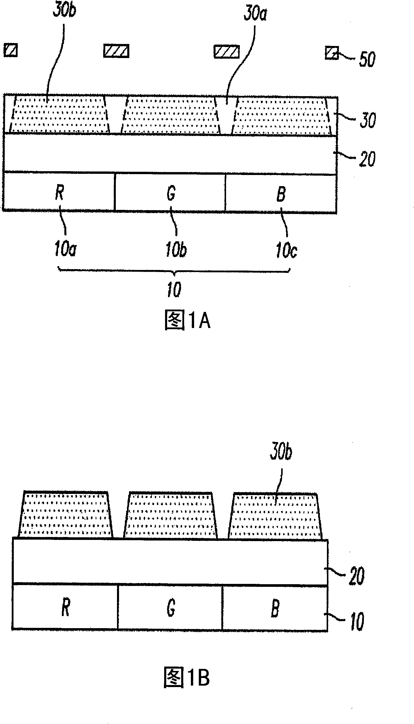
[0019] A plurality of metal wiring layers for electrically connecting circuit elements are formed on and / or over the semiconductor substrate. Circuit elements (eg, a photodiode and / or MOS transistors) are formed on and / or over the semiconductor substrate. Multiple interlayer dielectric layers may be formed to electrically isolate circuit elements and / or metal wiring layers. A color filter array 100 (eg, including red filter 100a, green filter 100b, and / or blue filter 100c) is formed on and / or over the upper interlayer dielectric layer. Flattening layer 200 is formed on and / or over color filter array 100 and compensates for height differences between different filters.

[0020] According to a...


PUM


Abstract

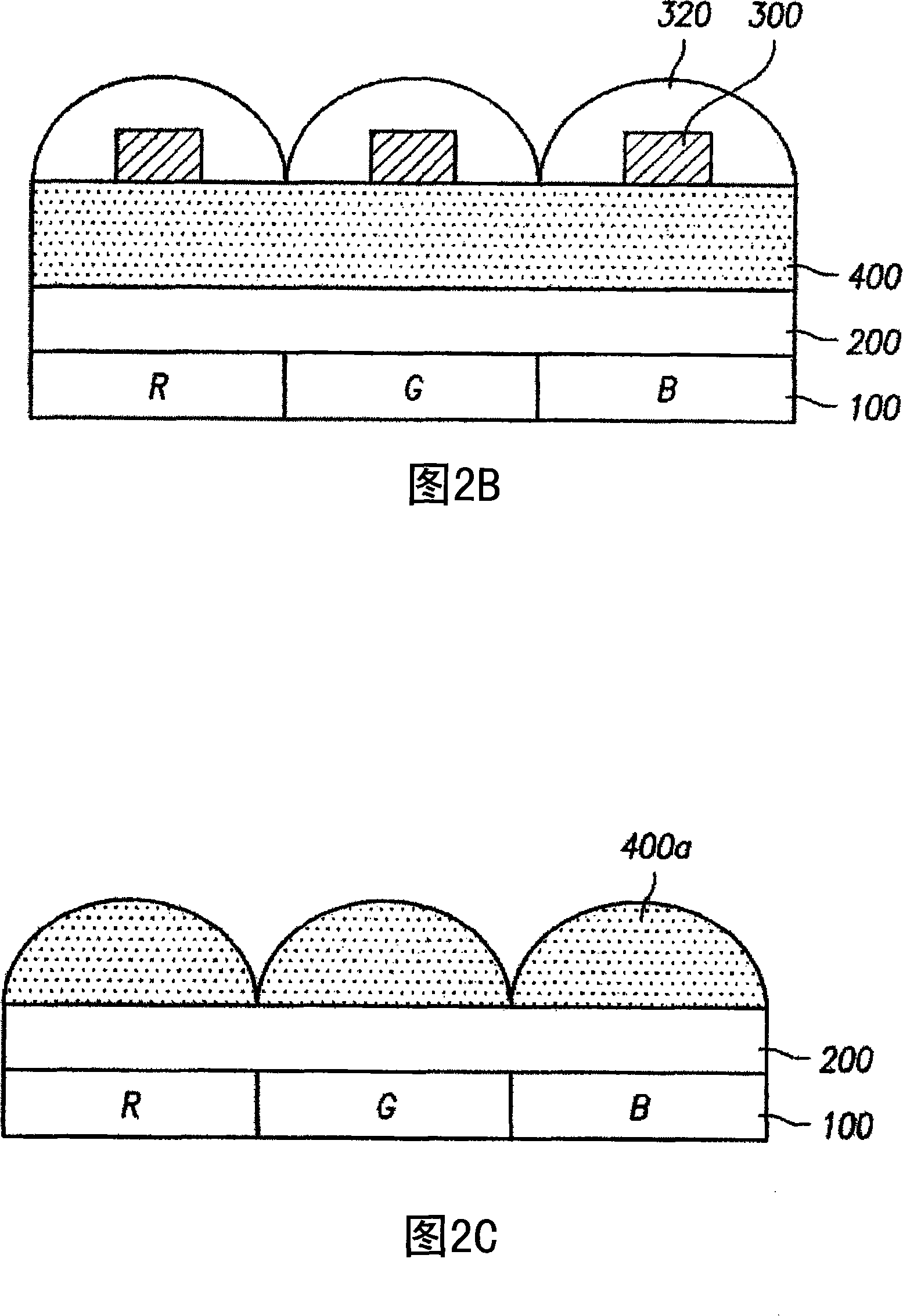
A microlens of a CMOS image sensor and a manufacturing method thereof, the method includes at least one of the following steps: forming a color filter array including a plurality of color filters on a semiconductor substrate. A flat layer is formed on and / or over the color filter array to compensate for height differences between the color filters. A silicon oxide layer is formed on and / or over the planarization layer. A plurality of photoresist patterns corresponding to the color filters are formed on and / or over the silicon oxide layer, wherein the photoresist patterns are separated from each other. A plurality of CxFy-based polymer bumps surrounding a plurality of photoresist patterns are formed using at least one process gas (eg, C5F8, CH2F2, Ar, and / or O2). Etching the plurality of polymer bumps, the plurality of photoresist patterns, and the oxide layer using an etch recipe having substantially the same etch selectivity between the plurality of polymer bumps, the plurality of photoresist patterns, and the silicon oxide layer silicon layer.

Description

[0001] This application claims priority from Korean Patent Application No. 10-2006-0072040 (filed on Jul. 31, 2006), the entire content of which is hereby incorporated by reference. technical field [0002] The invention relates to a microlens of a CMOS image sensor and a manufacturing method thereof. Background technique [0003] An image sensor is a device that receives light at a photodiode or phototransistor and uses an analog-to-digital converter (ADC) to convert the light into an electrical digital image signal. Two different image sensors are Complementary Metal Oxide Semiconductor (CMOS) devices and Charge Coupled Devices (CCD). CMOS devices can be used in small cameras with low power. In a CMOS device, a microlens (which may be exposed to air) focuses light onto a photodiode. A photodiode converts the collected light into an electrical signal. Multiple transistors can display the converted electrical signal as an image. [0004] A CMOS device may include a photo...

Claims


Application Information

Patent Timeline
IPC IPC(8): G03F7/00G03F1/00H01L27/14H01L27/146
CPCH01L27/14643H01L27/14621H01L27/14627H01L27/14685H01L27/146
Inventor 赵殷相
Owner DONGBU HITEK CO LTD
Learn More